Wafer graph display method, system and device and storage medium

A display method and wafer map technology, which is applied in the manufacture of electrical components, circuits, semiconductors/solid-state devices, etc., can solve problems such as inaccurate wafer extraction, achieve real-time display, achieve accurate positioning, and improve production efficiency.

Active Publication Date: 2021-06-18
SHENZHEN YUANMINGJIE TECH
View PDF6 Cites 0 Cited by
  • Summary
  • Abstract
  • Description
  • Claims
  • Application Information

AI Technical Summary

Problems solved by technology

[0004] The embodiment of the present application aims to solve the problem of determining the reference wafer from the wafer by naked eyes by providing a wafer map display method, system, device and storage medium Position parameter, the method of controlling the probe station to extract the wafer from the wafer according to the position parameter of the reference wafer is prone to the problem of inaccurate wafer extraction

Method used


Image

  • Wafer graph display method, system and device and storage medium
  • Wafer graph display method, system and device and storage medium
  • Wafer graph display method, system and device and storage medium

Examples


Embodiment Construction

[0046] In order to better understand the above-mentioned technical solutions, exemplary embodiments of the present disclosure will be described in more detail below with reference to the accompanying drawings. Although exemplary embodiments of the present disclosure are shown in the drawings, it should be understood that the present disclosure may be embodied in various forms and should not be limited by the embodiments set forth herein. Rather, these embodiments are provided for more thorough understanding of the present disclosure and to fully convey the scope of the present disclosure to those skilled in the art.

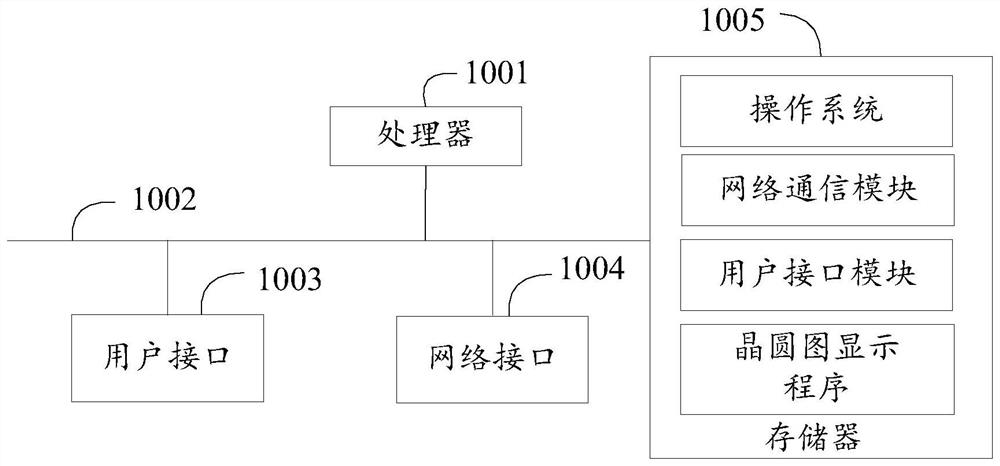
[0047] Such as figure 1 as shown, figure 1 It is a schematic structural diagram of the hardware operating environment involved in the solution of the embodiment of the present invention.

[0048] It should be noted, figure 1 A schematic structural diagram of the hardware operating environment of the device can be displayed for the wafer map.

[0049] Such as ...


PUM


Abstract

The invention discloses a wafer graph display method, system and device and a storage medium. The method comprises the following steps: displaying a wafer graph; when a wafer extraction event is received, setting a reference wafer, an extraction mode of the wafer and an extraction area on the wafer graph according to the wafer extraction event; acquiring position information of the reference wafer from the wafer graph; and taking the position information as an initial position, extracting qualified wafers in the wafers according to the extraction mode and the extraction area, and updating the displayed wafer graph according to the extracted wafers. In the wafer extraction link, real-time display of the wafer state information is realized, accurate positioning of the wafer is also realized, and the production efficiency of the wafer extraction link is greatly improved.

Description

technical field [0001] The invention relates to the technical field of semiconductor production, in particular to a wafer map display method, system, equipment and storage medium. Background technique [0002] In the production of semiconductor chips, a wafer (circular silicon wafer) with a diameter of a certain size is cut into several small chips. The small chip refers to the silicon wafer used in the manufacture of silicon semiconductor integrated circuits, also known as a wafer. [0003] At present, during the production of semiconductor chips, before controlling the probe station to extract the wafer from the wafer, it is often necessary to manually determine the position parameters of the reference wafer from the wafer with the naked eye, and then input the position parameters of the reference wafer into the probe. In the control system of the needle station, the wafer is extracted from the wafer by controlling the probe station. However, this method of determining t...

Claims


Application Information

Patent Timeline
Patent Type & Authority Applications(China)
IPC IPC(8): H01L21/68H01L21/67
CPCH01L21/68H01L21/67276H01L21/67259
Inventor 山无陵邹大卡黎理明黎理杰
Owner SHENZHEN YUANMINGJIE TECH
Why Eureka
Try Eureka