Micro LED chip mass transfer method and display backboard
A transfer method and chip transfer technology, applied in the direction of electrical components, electrical solid devices, circuits, etc., can solve the problems of position deviation, difficult and effective electrical connection of MicroLED chips, etc., and achieve effective electrical connection, high-precision mass transfer, high The effect of efficiency
- Summary
- Abstract
- Description
- Claims
- Application Information
AI Technical Summary
Problems solved by technology
Method used
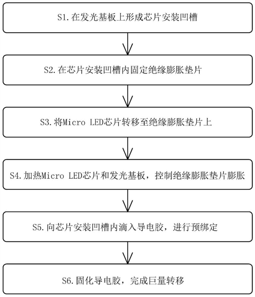
Image

Examples
Embodiment Construction
[0066] In order to make the object, technical solution and advantages of the present invention more clear and definite, the present invention will be further described in detail below with reference to the accompanying drawings and examples. It should be understood that the specific embodiments described here are only used to explain the present invention, not to limit the present invention.
[0067] In the description of the present invention, it should be understood that the orientation or positional relationship indicated by the terms "center", "upper", "lower", "front", "rear", "left", "right" etc. are based on The orientations or positional relationships shown in the drawings are only for the convenience of describing the present invention and simplifying the description, and do not indicate or imply that the referred devices or components must have a specific orientation, be constructed and operated in a specific orientation, and therefore cannot be understood as Limitat...
PUM
 Abstract
Description
Claims
Application Information
 - R&D
- Intellectual Property
- Life Sciences
- Materials
- Tech Scout
- Unparalleled Data Quality
- Higher Quality Content
- 60% Fewer Hallucinations
Browse by: Latest US Patents, China's latest patents, Technical Efficacy Thesaurus, Application Domain, Technology Topic, Popular Technical Reports.
© 2025 PatSnap. All rights reserved.Legal|Privacy policy|Modern Slavery Act Transparency Statement|Sitemap|About US| Contact US: help@patsnap.com