Light source positioning device and semiconductor optical measuring device

A positioning device and semiconductor technology, which is applied in the direction of transmitting sensing components, measuring devices, instruments, etc. using optical devices, can solve the problems of small reserved space, SELamp light concentration, and affecting personnel operations, etc., to achieve easy replacement and ensure concentration Lighting and accuracy-enhancing effects

Active Publication Date: 2022-06-03
YANGTZE MEMORY TECH CO LTD
View PDF0 Cites 0 Cited by
  • Summary
  • Abstract
  • Description
  • Claims
  • Application Information

AI Technical Summary

Problems solved by technology

[0002] In the prior art semiconductor optical measurement, the light source device (such as SE Lamp) for optical measurement is replaced, and the orientation mark (Lamp notch) of the light source device is roughly placed in the direction parallel to the EFEM based on the personal experience of the operator. In this case It is easy to cause the light concentration of SE Lamp, which will lead to the adjustment of optical path and product measurement in the later stage; at the same time, because of the small reserved space, it will affect the operation of personnel

Method used


Image

  • Light source positioning device and semiconductor optical measuring device
  • Light source positioning device and semiconductor optical measuring device

Examples


Embodiment Construction

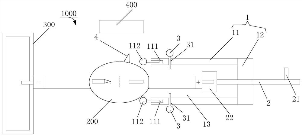
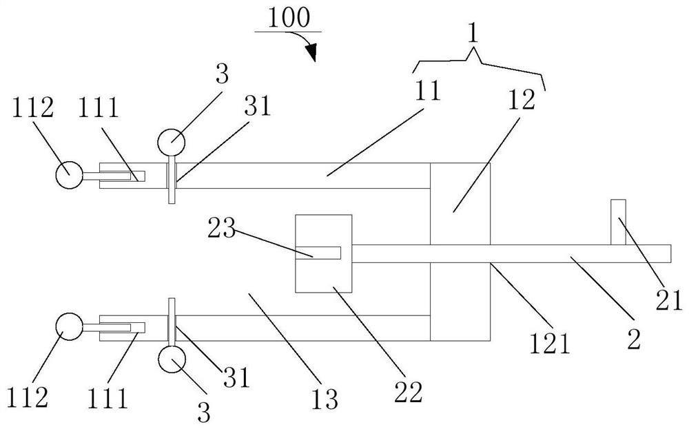
[0027] A light source positioning device 100 for semiconductor optical measurement proposed by the present invention will be further described in detail below with reference to the accompanying drawings and specific embodiments.

[0028] The semiconductor optical measurement device 300 is provided with a light source device 200 for semiconductor optical measurement. The light source device 200 may be a laser or the like, and the light source device 200 has a positioning mark 4. The positioning mark 4 may be formed as a protruding bump, for example, a In the shape of a protruding pyramid or cone, when the light source device 200 is installed on the semiconductor optical measuring device 300 , the orientation mark 4 needs to face a specific direction to ensure the stability of subsequent optical path adjustment and measurement. The installation of the light source device 200 in the prior art is only based on the personal experience of the operator, which leads to inaccurate insta...


PUM


Abstract

This invention discloses a light source positioning device for semiconductor optical measurement and a semiconductor optical measurement device. The housing includes a positioning piece and a fixing piece for fixed connection with the semiconductor optical measuring equipment; a positioning rod, the positioning rod is movably installed on the positioning piece and the positioning One end of the rod extends into the installation cavity, and one end of the positioning rod extending into the installation cavity is provided with a base. When the optical measuring device is used, the light source device is installed in place and the positioning mark of the light source device is located at the positioning position. The light source positioning device can improve the installation accuracy of the light source device, and ensure the light concentration of the light source device and the measurement stability of the optical measuring equipment.

Description

technical field [0001] The present invention relates to the technical field of semiconductors, in particular to a light source positioning device for semiconductor optical measurement and a semiconductor optical measurement device having the same. Background technique [0002] In the prior art semiconductor optical measurement, the light source device (such as SE Lamp) for optical measurement is replaced, and the orientation mark (Lamp notch) of the light source device is placed roughly parallel to the EFEM direction according to the operator's personal experience. It is easy to lead to the concentrating of the SE Lamp, which will lead to the later adjustment of the optical path and product measurement; at the same time, because the reserved space is small, it will affect the operation of personnel. SUMMARY OF THE INVENTION [0003] The purpose of the present invention is to provide a light source positioning device for semiconductor optical measurement, which can improve ...

Claims


Application Information

Patent Timeline
Patent Type & Authority Patents(China)
IPC IPC(8): G01D5/26F16M11/04
CPCG01D5/264F16M11/04
Inventor 周毅梁亚军
Owner YANGTZE MEMORY TECH CO LTD
Why Eureka
Try Eureka