


Quick Research
Generate reliable direction feasibility study reports for your R&D in just a few steps.

Technical Q&A
Discover and master advanced knowledge NOW. Basics, ideas, possibilities, all at once.

Find Solutions
As an expert in R&D theories, this can generate solutions to your technical problems instantly.

Evaluate Feasibility
Analyze your overall solution with one click, know your potential R&D risks in advance.

Monitor Landscape
Get weekly tech updates, stay abreast of the latest tech innovations and key insights.
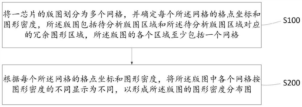
Method and device for analyzing graph density of chip and electronic equipment
A technology of pattern density and analysis method, applied in electrical digital data processing, computer-aided design, special data processing applications, etc., can solve the problems of reducing product yield, reducing the efficiency of layout pattern density analysis, etc.
- Summary
- Abstract
- Description
- Claims
- Application Information
AI Technical Summary
Problems solved by technology
Method used
Image

Examples
Embodiment Construction
[0045] The specific implementation manner of the present invention will be described in more detail below with reference to schematic diagrams. The advantages and features of the present invention will be more apparent from the following description. It should be noted that all the drawings are in a very simplified form and use imprecise scales, and are only used to facilitate and clearly assist the purpose of illustrating the embodiments of the present invention.
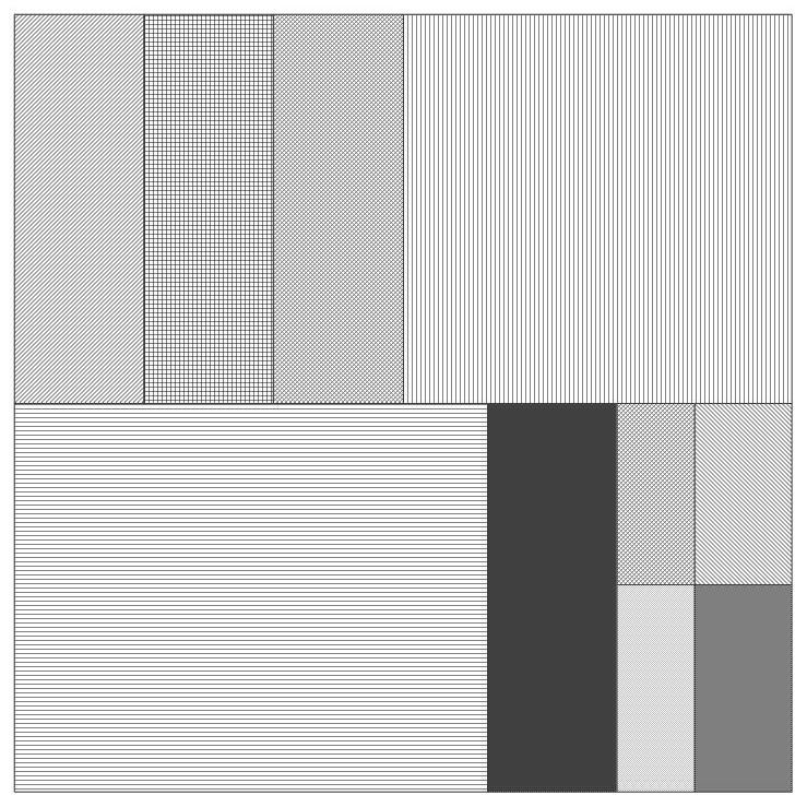
[0046] As mentioned in the background, in the prior art, the method of adding redundant patterns is to use manual or software to automatically fill redundant metals to improve the uniformity of layout pattern density. Based on this, the current conventional pattern density inspection method only uses simulation software to find areas with too high or too low pattern density in the layout pattern, but it cannot allow researchers to directly view the overall distribution of the pattern density of the layout pattern a...
PUM
 Abstract
Description
Claims
Application Information
 - R&D Engineer
- R&D Manager
- IP Professional
- Industry Leading Data Capabilities
- Powerful AI technology
- Patent DNA Extraction
Browse by: Latest US Patents, China's latest patents, Technical Efficacy Thesaurus, Application Domain, Technology Topic, Popular Technical Reports.
© 2024 PatSnap. All rights reserved.Legal|Privacy policy|Modern Slavery Act Transparency Statement|Sitemap|About US| Contact US: help@patsnap.com