Semiconductor device and method of forming the same
A semiconductor and device technology, applied in the field of semiconductor devices and their formation, can solve the problems of difficult preparation and inflexible process, and achieve the effects of improving process constraints, increasing manufacturing efficiency, and reducing manufacturing difficulty
- Summary
- Abstract
- Description
- Claims
- Application Information
AI Technical Summary
Problems solved by technology
Method used
Image

Examples
preparation example Construction
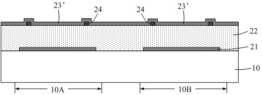
[0038] As mentioned in the background, for the resonant structure provided with the metal ring and the mass load layer, the preparation process is difficult to be compatible, and the preparation method still needs to be improved. For details, please refer to figure 1 and figure 2 As shown, a method for forming a semiconductor device includes the following steps, for example.
[0039] In the first step, the lower electrode layer 21 is formed on the resonance region of the substrate 10 . figure 1 It schematically shows the first resonant region 10A and the second resonant region 10B where resonant structures need to be formed, and the lower electrode layer 21 is formed on both the first resonant region 10A and the second resonant region 10B.
[0040] In the second step, the piezoelectric layer 22 is formed on the substrate 10 .
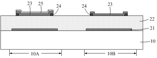
[0041] In the third step, a metal ring 24 is formed on the piezoelectric layer 22 in the resonance area. figure 1 In other words, metal rings 24 a...
Embodiment 1
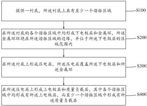
[0052] In this embodiment, a method for forming a semiconductor device is explained by taking a part of the resonant region provided with a mass-loaded layer and another part of the resonant region not provided with a mass-loaded layer as an example.
[0053] In step S100, specifically refer to Figure 4 As shown, a substrate 100 is provided, and there is at least one resonant region on the substrate 100, and the resonant region is a region for forming a resonant structure. In this embodiment, only two resonant regions are shown as examples for explanation, for example Figure 4 As shown, the substrate 100 has a first resonant region 100A and a second resonant region 100B.
[0054] Wherein, the substrate 100 can be correspondingly adjusted according to the specific application of the formed semiconductor device. For example, the semiconductor device can be a bulk acoustic wave filter (bulk acoustic wave, BAW), at this time, the substrate can include multiple Bragg reflection...
Embodiment 2
[0084] The difference from Embodiment 1 is that in this embodiment, the description is made for the case where mass load layers with different thicknesses are provided for different resonant structures of a semiconductor device.
[0085] specific reference Figure 9 As shown, the resonant structure of the first resonant region 100A of the semiconductor device and the resonant structure of the second resonant region 100B are both formed with mass load layers. Wherein, the thickness of the mass-loaded layer 250a in the first resonant region 100A is different from the thickness of the mass-loaded layer 250b in the second resonant region 100B, so that the resonance of the resonant structure in the first resonant region 100A The frequency is different from the resonance frequency of the resonance structure in the second resonance region 100B. In this embodiment, the thickness of the mass load layer 250a in the first resonant region 100A is greater than the thickness of the mass lo...
PUM
| Property | Measurement | Unit |
|---|---|---|
| thickness | aaaaa | aaaaa |
| thickness | aaaaa | aaaaa |
Abstract
Description
Claims
Application Information
 - R&D
- Intellectual Property
- Life Sciences
- Materials
- Tech Scout
- Unparalleled Data Quality
- Higher Quality Content
- 60% Fewer Hallucinations
Browse by: Latest US Patents, China's latest patents, Technical Efficacy Thesaurus, Application Domain, Technology Topic, Popular Technical Reports.
© 2025 PatSnap. All rights reserved.Legal|Privacy policy|Modern Slavery Act Transparency Statement|Sitemap|About US| Contact US: help@patsnap.com