Leakage protection PCB suitable for automatic welding, and welding process thereof
An automatic welding and PCB board technology, applied in printed circuits connected with non-printed electrical components, switches with multiple unbalanced current/voltage effects, emergency protection devices, etc.
- Summary
- Abstract
- Description
- Claims
- Application Information
AI Technical Summary
Problems solved by technology
Method used
Image
Examples
Embodiment 1
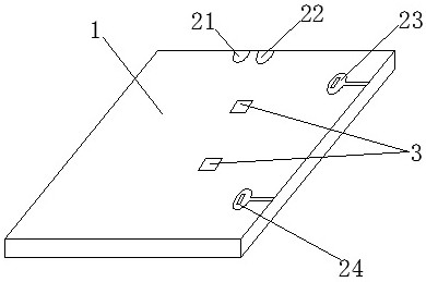
[0027] This embodiment describes a leakage protection PCB board suitable for automatic welding, such as figure 1 As shown, it includes a PCB board main body 1, and a positioning hole 3 for clamping and fixing itself is provided in the middle part of the PCB board main body 1, and at least two plane soldering pads are arranged on the surface of the PCB board, and the at least two plane soldering pads are arranged on the surface of the PCB board. The pads include a first pad 21 and a second pad 22 connected to the leads of the transformer.
[0028] The at least two planar pads also include a third pad 23 and a fourth pad 24, and the third pad 23 and the fourth pad 24 are used to connect the live wire and the neutral wire respectively.
Embodiment 2
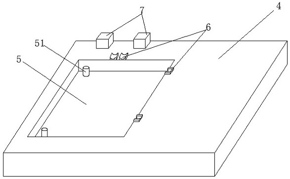
[0030] This embodiment has described a kind of leakage protection PCB board welding process that is applicable to automatic welding, as figure 1 As shown, a plurality of planar pads are arranged on the PCB main body 1 of the leakage protection PCB board, and corresponding to the plurality of planar pads are respectively connected to lead wires or input phase lines. 1 for positioning and a plurality of guide grooves 6 are provided on the surface of the fixture at the edge of the PCB board main body 1 corresponding to the lead wire or the input phase line.
[0031] Optionally, the plurality of planar pads include a first pad 21 and a second pad 22 connected to leads of the transformer. The plurality of planar pads also includes a third pad 23 and a fourth pad 24, and the third pad 23 and the fourth pad 24 are used to connect the live wire and the neutral wire respectively.
[0032] In order to facilitate the rapid positioning of the PCB board main body 1, such as figure 2 As ...
PUM
 Abstract
Description
Claims
Application Information
 - R&D
- Intellectual Property
- Life Sciences
- Materials
- Tech Scout
- Unparalleled Data Quality
- Higher Quality Content
- 60% Fewer Hallucinations
Browse by: Latest US Patents, China's latest patents, Technical Efficacy Thesaurus, Application Domain, Technology Topic, Popular Technical Reports.
© 2025 PatSnap. All rights reserved.Legal|Privacy policy|Modern Slavery Act Transparency Statement|Sitemap|About US| Contact US: help@patsnap.com


