Epitaxial wafer of light-emitting diode and its preparation method

A technology of light-emitting diodes and epitaxial wafers, applied in semiconductor devices, electrical components, circuits, etc., can solve the problems of reducing the electric injection efficiency and luminous efficiency of deep ultraviolet light-emitting diodes, the deterioration of AlGaN crystal quality, and the decline of carrier mobility. , to achieve the effect of improving the electric injection efficiency and luminous efficiency, reducing the self-compensation effect, and facilitating the mobility

Active Publication Date: 2022-04-15
HC SEMITEK ZHEJIANG CO LTD
View PDF7 Cites 0 Cited by
  • Summary
  • Abstract
  • Description
  • Claims
  • Application Information

AI Technical Summary

Problems solved by technology

[0004] In deep ultraviolet light-emitting diodes, in order to achieve high carrier concentration, the concentration of dopants is usually increased, but this will easily lead to poor AlGaN crystal quality, defects (mainly including vacancies and their complexes, impurities, dislocations, etc.) The density increases, the compensation effect intensifies, and the carrier mobility decreases, which leads to a decrease in the conductivity of the n-type layer and reduces the electrical injection efficiency and luminous efficiency of deep ultraviolet light-emitting diodes.

Method used


Image

  • Epitaxial wafer of light-emitting diode and its preparation method
  • Epitaxial wafer of light-emitting diode and its preparation method
  • Epitaxial wafer of light-emitting diode and its preparation method

Examples


Embodiment Construction

[0030] In order to make the purpose, technical solution and advantages of the present disclosure clearer, the implementation manners of the present disclosure will be further described in detail below in conjunction with the accompanying drawings.

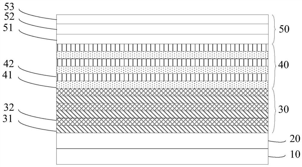
[0031] figure 1 It is a schematic structural diagram of an epitaxial wafer of a light emitting diode provided by an embodiment of the present disclosure. Such as figure 1 As shown, the epitaxial wafer includes a substrate 10 and an AlN buffer layer 20 , an n-type layer 30 , a multi-quantum well layer 40 and a p-type layer 50 sequentially formed on the substrate 10 .

[0032] Wherein, the n-type layer 30 includes a superlattice structure formed by alternately stacking multiple InN layers 31 and multiple AlInGaN layers 32 , and the AlInGaN layers 32 are doped with Si.

[0033] By adopting a superlattice structure formed by alternate lamination of multiple InN layers and multiple AlInGaN layers as the n-type layer, the AlInGaN layer...


PUM

PropertyMeasurementUnit
thicknessaaaaaaaaaa
thicknessaaaaaaaaaa
temperatureaaaaaaaaaa

Abstract

The disclosure provides an epitaxial wafer of a light emitting diode and a preparation method thereof, which belong to the technical field of optoelectronic manufacturing. The epitaxial wafer includes a substrate and an AlN buffer layer, an n-type layer, a multi-quantum well layer and a p-type layer formed sequentially on the substrate, wherein the n-type layer includes a plurality of InN layers and a plurality of AlInGaN A superlattice structure formed by alternating layers, the AlInGaN layer is doped with Si, Si and In in the AlInGaN layer form a Si-In co-doped structure, and the Si-In co-doped structure can effectively suppress the formation of deep main centers, Thereby reducing the self-compensation effect and improving the mobility of carriers. InN materials also have good electron transport performance, which is also conducive to the improvement of carrier mobility, thereby improving the conductivity of the n-type layer and improving the deep ultraviolet Electric injection efficiency and luminous efficiency of light-emitting diodes.

Description

technical field [0001] The disclosure relates to the technical field of optoelectronic manufacturing, in particular to an epitaxial wafer of a light emitting diode and a preparation method thereof. Background technique [0002] Light Emitting Diode (English: Light Emitting Diode, referred to as: LED), as a very influential new product in the optoelectronics industry, has the characteristics of small size, long service life, colorful colors, and low energy consumption. It is widely used in lighting, display screens , signal lights, backlight, toys and other fields. The core structure of the LED is the epitaxial wafer, and the production of the epitaxial wafer has a great influence on the photoelectric characteristics of the LED. [0003] Epitaxial wafers generally include buffer layers, n-type layers, multiple quantum well layers, and p-type layers. The n-type layer in the epitaxial wafer of the deep ultraviolet light-emitting diode is usually an AlGaN layer. [0004] In d...

Claims


Application Information

Patent Timeline
Patent Type & Authority Patents(China)
IPC IPC(8): H01L33/04H01L33/06H01L33/12H01L33/14H01L33/32H01L33/00
CPCH01L33/12H01L33/06H01L33/04H01L33/32H01L33/325H01L33/14H01L33/007
Inventor 丁涛龚程成尹涌梅劲
Owner HC SEMITEK ZHEJIANG CO LTD
Why Eureka
Try Eureka