Chemical vapor deposition method for preparing silicon carbide composite coating on single crystal silicon or polycrystalline silicon

A technology of chemical vapor deposition and composite coating, which is applied in the direction of coating, gaseous chemical plating, metal material coating technology, etc., can solve the problems of poor bonding between coating and substrate, thermal expansion coefficient mismatch, etc., to achieve good bonding, Dense structure, smooth surface effect

Active Publication Date: 2021-09-24
INST OF METAL RESEARCH - CHINESE ACAD OF SCI
View PDF8 Cites 0 Cited by
  • Summary
  • Abstract
  • Description
  • Claims
  • Application Information

AI Technical Summary

Problems solved by technology

[0006] The purpose of the present invention is to provide a chemical vapor deposition method for preparing a silicon carbide composite coating on single crystal silicon or polycrystalline silicon to solve the problem of poor bonding between the coating and the substrate due to thermal expansion coefficient mismatch

Method used


Image

  • Chemical vapor deposition method for preparing silicon carbide composite coating on single crystal silicon or polycrystalline silicon
  • Chemical vapor deposition method for preparing silicon carbide composite coating on single crystal silicon or polycrystalline silicon

Examples


Embodiment 1

[0035] In the present embodiment, the chemical vapor deposition method of the silicon carbide composite coating is prepared on single crystal silicon is as follows:

[0036](1) The single crystal silicon substore is 50 min in deionized water and acetone, respectively, and then placed in hydrofluoric acid having a concentration of 5 wt%, and places the silicon base in the reaction chamber;

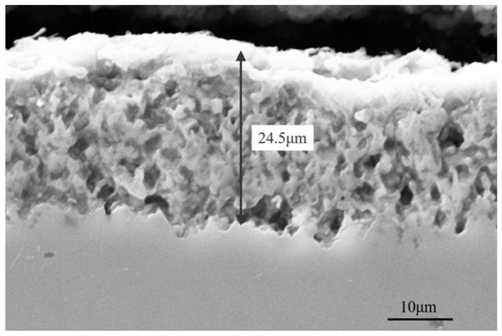
[0037] (2) Preparation of a porous silicon layer on a silicon substrate, an access H 2 And Ar, H 2 The flow rate is 200 sccm, the Ar flow is 1500 sccm, the etching temperature is 1200 ° C, the working pressure is 200 Pa, the etching time is 30 min, the thickness of the porous silicon layer is 24.5 μm, see figure 1 ;

[0038] (3) Deposit a thin layer of SiOc buffer layer on the porous silicon layer, HMDSO liquid flow rate is 0.3 g / min, h 2 The flow rate of Ar is 200 Sccm, 3000 sccm, deposition temperature 1050 ° C, the working pressure is 300 Pa, deposition time 30 min, and the thickness of th...

Embodiment 2

[0044] In the present embodiment, the chemical vapor deposition method of the silicon carbide composite coating is prepared on the polysilicon is as follows:

[0045] (1) The polysilicon base is applied in deionized water and acetone, respectively, and then placed in hydrofluoric acid having a concentration of 5 wt%, placing the silicon substrate in the reaction chamber;

[0046] (2) Preparation of a porous silicon layer on a silicon substrate, an access H 2 And Ar, H 2 The flow rate 300sccm, the Ar flow rate is 3000 sccm, the etching temperature is 1250 ° C, the working pressure is 400 Pa, the etching time is 15 min, the thickness of the porous silicon layer is 12.5 μm;

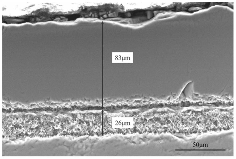
[0047] (3) Deposit a layer of SiOC buffer layer on the porous silicon layer, HMDSO liquid flow rate is 0.6 g / min, h 2 The flow rate of Arccm, 5000 sccm, deposition temperature is 1100 ° C, the working pressure is 600Pa, the deposition time is 40 min, and the thickness of the buffer layer is 1.8 μm;

[0048] (4...


PUM

PropertyMeasurementUnit
thicknessaaaaaaaaaa
thicknessaaaaaaaaaa
thicknessaaaaaaaaaa

Abstract

The invention belongs to the field of coating preparation, and in particular relates to a chemical vapor deposition method for preparing a silicon carbide composite coating on single crystal silicon or polycrystalline silicon. Using metal organic compound chemical vapor deposition (MOCVD) system, select liquid raw material hexamethyldisilane (HMDS) or hexamethyldisiloxane (HMDSO), H 2 And Ar gas system, the working pressure is 10-1000Pa, and the temperature is 900-1350℃. Before depositing the coating, the monocrystalline silicon or polycrystalline silicon substrate is pretreated to form a porous silicon layer, and then the coating is deposited on the porous silicon layer. The composite coating starts from the Si substrate and is sequentially porous silicon layer, buffer layer, SiOC layer and pure SiC layer. The silicon carbide composite coating deposited by the method of the invention has the characteristics of compact structure, no obvious cracks, good combination with the matrix, and the like. The composite coating designed by the invention skillfully coordinates the stress matching problem between the SiC coating and the Si substrate, and the thickness of the composite coating prepared by the method can exceed 1.5mm.

Description

Technical field [0001] The present invention belongs to the field of coating preparation, and more particularly to a chemical vapor deposition method for preparing a silicon carbide composite coating on single crystal silicon or polysilicon. Background technique [0002] Dry etch is the main technical path manufacturing of chip, and commonly used etching gases include sf 6 CF 4 , C 4 Fly 8 And O 2 Wait. During the etching process, the main function of the fluorine-containing gas is chemically reacted by ionizing fluoride ions, fluoride ions and silicon-silicon carbide substrates, to generate SIF 4 Gas and enclose etching of silicon atoms. At present, since the silicon wafer is also more silicon materials, it is necessary to effectively protect this part of the silicon material in order to improve the service life of the stage. [0003] The silicon carbide material has a large width of the breakdown, the intensity of the breakdown electric field is high, the inertia is high, and t...

Claims


Application Information

Patent Timeline
Patent Type & Authority Patents(China)
IPC IPC(8): C23C16/02C23C16/30C23C16/32
CPCC23C16/0227C23C16/0272C23C16/30C23C16/325
Inventor 唐明强刘厚盛崔新宇王吉强沈艳芳熊天英
Owner INST OF METAL RESEARCH - CHINESE ACAD OF SCI
Why Eureka
Try Eureka