A kind of mems optical switch automatic scanning device and method
An automatic scanning and optical switching technology, applied in the field of optical communication, can solve the problems of performance degradation, micromirrors susceptible to dust and other particles, channel voltage parameter deviation, etc., to achieve high-speed production debugging, improve maintenance and use efficiency.
- Summary
- Abstract
- Description
- Claims
- Application Information
AI Technical Summary
Problems solved by technology
Method used
Image
Examples
Embodiment Construction
[0022] The technical solutions in the embodiments of the present application will be clearly and completely described below with reference to the drawings in the embodiments of the present application. Obviously, the described embodiments are only a part of the embodiments of the present application, but not all of the embodiments. Based on the embodiments in the present application, all other embodiments obtained by those of ordinary skill in the art without creative efforts shall fall within the protection scope of the present application.
[0023] The content of the present invention will be further elaborated below in conjunction with the accompanying drawings and embodiments, but it is not intended to limit the present invention.
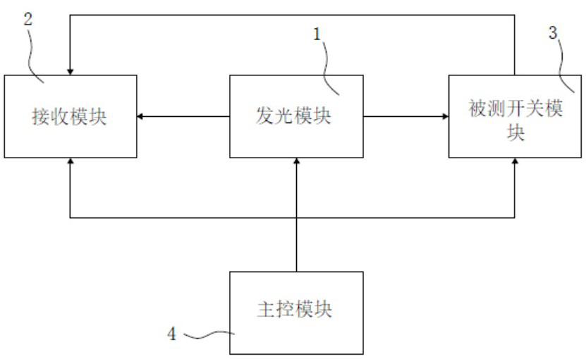
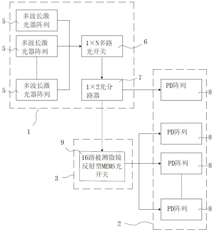
[0024] refer to Figure 1-Figure 2 , the present application provides a MEMS optical switch automatic scanning device, including four components: a light-emitting module 1, a receiving module 2, a measured light switch module 3 and a main contr...
PUM
 Abstract
Description
Claims
Application Information
 - R&D Engineer
- R&D Manager
- IP Professional
- Industry Leading Data Capabilities
- Powerful AI technology
- Patent DNA Extraction
Browse by: Latest US Patents, China's latest patents, Technical Efficacy Thesaurus, Application Domain, Technology Topic, Popular Technical Reports.
© 2024 PatSnap. All rights reserved.Legal|Privacy policy|Modern Slavery Act Transparency Statement|Sitemap|About US| Contact US: help@patsnap.com


