Electric on-off test method for double-sided substrate

A double-sided substrate, on-off test technology, used in semiconductor/solid-state device testing/measurement, circuits, electrical components, etc.

Active Publication Date: 2021-03-16
珠海天成先进半导体科技有限公司
View PDF16 Cites 1 Cited by
  • Summary
  • Abstract
  • Description
  • Claims
  • Application Information

AI Technical Summary

Problems solved by technology

[0004] In order to solve the problems existing in the prior art, the present invention provides an electrical on-off testing method for double-sided substrates, which solves the electrical on-off testing problem of ultra-thin large-size silicon transfer substrate wafers, and is comparable to existing commercial equipment. Compatible, suitable for automated mass production testing

Method used


Image

  • Electric on-off test method for double-sided substrate
  • Electric on-off test method for double-sided substrate
  • Electric on-off test method for double-sided substrate

Examples


Embodiment

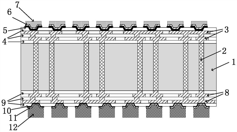
[0034] Such as figure 1 As shown, the TSV conductive via 2 penetrating the silicon substrate 1 realizes the electrical connection between the upper and lower surfaces of the silicon substrate 1 . The front metal wiring 3 is arranged for horizontal electrical connection on the upper surface of the silicon substrate 1. The number of layers of the front metal wiring 3 is at least one layer. When the front metal wiring 3 is multi-layered, the front metal wiring 3 of each layer passes through the front The inter-metal dielectric 4 is electrically insulated, and the electrical connection between the front metal wirings 3 of each layer is realized through the connection holes between each layer. The front bumps 7 are electrically connected to the front metal wiring 3 through the front under bump metallurgy (UBM) 6 . Correspondingly, the back metal wiring 8 is arranged for horizontal electrical connection on the lower surface of the silicon substrate 1, and the number of layers of th...


PUM

PropertyMeasurementUnit
thicknessaaaaaaaaaa

Abstract

The invention discloses an electric on-off test method for a double-sided substrate, and the method comprises the steps: 1, enabling a front electroplating seed layer not to be etched in a preparationprocess of the double-sided substrate, and reserving the front electroplating seed layer; 2, completing a back surface process of the double-sided substrate on the double-sided substrate with the front surface electroplating seed layer reserved, etching the back surface electroplating seed layer, then performing a first single-sided probe test on back surface bumps of the double-sided substrate,and measuring an electrical on-off connection relationship between every two back surface bumps; 3, etching the front electroplating seed layer in an area outside the front bumps, performing a secondsingle-sided probe test on the front bumps of the double-sided substrate, and measuring an electric on-off connection relationship between every two front bumps; and 4, combining the first single-sided probe test result in the step 2 and the second single-sided probe test result in the step 3 to obtain an electrical connection test result between the bumps on the front and back surfaces of the double-sided substrate. The electric on-off test problem of a silicon switching substrate wafer is solved, and the method is suitable for automatic mass production test.

Description

technical field [0001] The invention belongs to the technical field of advanced electronic packaging, in particular to an electric continuity test method for a double-sided substrate. Background technique [0002] Over the years, the technological development of packaging substrates including ceramic substrates and organic substrates has been far behind integrated circuit IC chips. At present, most advanced integrated circuit IC chips use the form of external pins of micro-bump arrays, and the number of pins is often thousands. , the pin density increases, and at the same time, the large size of the IC chip and the low-K dielectric layer pose a great challenge to traditional packaging substrates such as ceramic substrates and organic substrates with poor flatness and obvious thermal mismatch. TSV silicon interposer (Si Interposer) is introduced as a bridge between advanced integrated circuit IC chips and traditional packaging substrates such as ceramic substrates and organic...

Claims


Application Information

Patent Timeline
Patent Type & Authority Applications(China)
IPC IPC(8): H01L21/66
CPCH01L22/14H01L22/20
Inventor 李宝霞
Owner 珠海天成先进半导体科技有限公司
Why Eureka
Try Eureka