Glass Photonic Crystal Selective Absorber Based on dbs Algorithm
A photonic crystal and selective technology, applied in mirrors, instruments, optics, etc., can solve the problem of poor radiation cooling effect of devices and achieve the effect of improving absorption spectrum
- Summary
- Abstract
- Description
- Claims
- Application Information
AI Technical Summary
Problems solved by technology
Method used
Image
Examples
Embodiment Construction
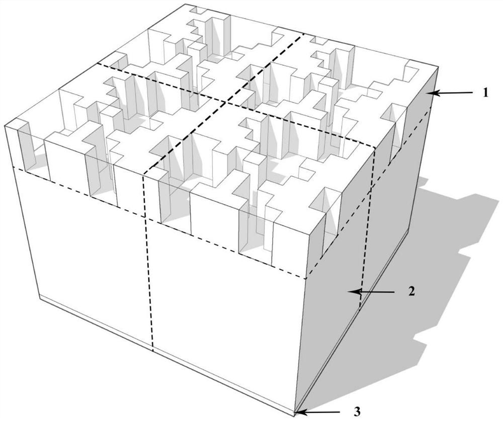
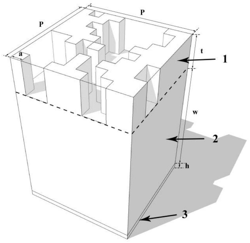
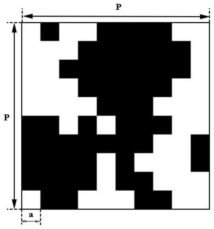
[0025] The present invention proposes a glass photonic crystal selective absorber based on the DBS algorithm, and its periodic three-dimensional structure schematic diagram is as follows figure 1 As shown, the schematic diagram of the three-dimensional structure of a unit in the periodic structure is shown in figure 2 As shown, it includes an optimized selective absorption region 1, an absorption layer 2, and a reflection layer 3.
[0026] The material of the optimized selective absorption region 1 is glass photonic crystal, and the thickness of the optimized selective absorption region 1 is t=3 μm; the material of the described absorption layer 2 is silicon dioxide, and the thickness of the absorption layer 2 is w=11 μm, the material of the reflective layer 3 is silver, and the thickness is h=0.5 μm.
[0027] Silver is widely used as an ideal conductor material in the infrared band, so we coat a layer of silver film on the bottom of the silicon dioxide absorbing layer, so t...
PUM
| Property | Measurement | Unit |
|---|---|---|
| size | aaaaa | aaaaa |
| thickness | aaaaa | aaaaa |
| thickness | aaaaa | aaaaa |
Abstract
Description
Claims
Application Information
 - Generate Ideas
- Intellectual Property
- Life Sciences
- Materials
- Tech Scout
- Unparalleled Data Quality
- Higher Quality Content
- 60% Fewer Hallucinations
Browse by: Latest US Patents, China's latest patents, Technical Efficacy Thesaurus, Application Domain, Technology Topic, Popular Technical Reports.
© 2025 PatSnap. All rights reserved.Legal|Privacy policy|Modern Slavery Act Transparency Statement|Sitemap|About US| Contact US: help@patsnap.com


