Test signal parallel loading conversion circuit and system-on-chip
A technology for testing signals and converting circuits, which is applied in the direction of measuring electricity, measuring electrical variables, and electronic circuit testing. The effect of reducing the cost of testing
- Summary
- Abstract
- Description
- Claims
- Application Information
AI Technical Summary
Problems solved by technology
Method used
Image

Examples
Embodiment 1
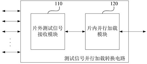
[0027] figure 1 A structural diagram of a test signal parallel loading conversion circuit provided for Embodiment 1 of the present invention. This embodiment is applicable to functional testing of each IP core included in the chip by multiplexing structural test pins. Condition. Such as figure 1 As shown, the test signal parallel loading conversion circuit includes: a connected off-chip test signal receiving module 110 and an on-chip parallel loading module 120 .
[0028] The off-chip test signal receiving module 110 is configured to receive parallel test signals from multiple scan test pins at an off-chip clock rate, and transmit the parallel test signals to the on-chip parallel loading module at an on-chip clock rate.
[0029] In this embodiment, the test signal parallel load conversion circuit can be configured on the SOC and connected to each scan test pin on the SOC, and the scan test pin can refer to a GPIO (General Purpose Input Output, General Purpose Input Output) c...
Embodiment 2
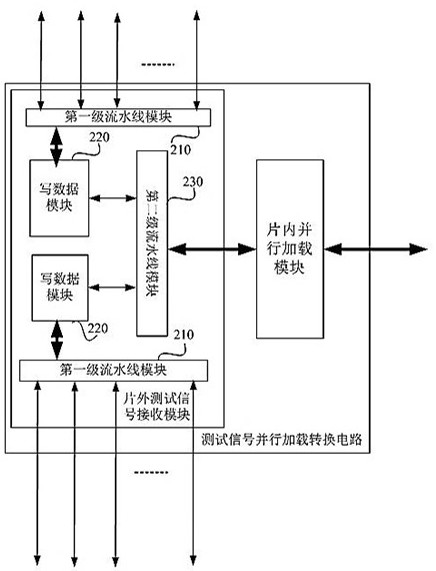
[0040] Figure 2a It is a structural diagram of a test signal parallel loading conversion circuit provided by Embodiment 2 of the present invention, as shown in Figure 2a As shown, in this embodiment, the off-chip test signal receiving module may include: at least one first-stage pipeline module 210, at least one write data module 220 correspondingly connected to each first-stage pipeline module 210, and each write data module 220. The second-stage pipeline module 230 connected to the module 220;
[0041] The first-stage pipeline module 210 is configured to receive parallel test signals from a plurality of scan test pins at an external clock rate, and output the parallel test signals to the write data module 220;
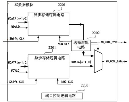
[0042] The write data module 220 is used to convert the parallel test signal of the off-chip clock rate into the parallel test signal of the on-chip clock rate after the data integration of the parallel test signal is carried out to the second-stage pipeline modul...
Embodiment 3
[0072] For example, 3 is a SoC in the third embodiment of the present invention, the SoC includes: NOC router 310, at least one IP core 320, multiple scan test pins 330, and parallel loading of test signals as described in any embodiment of the present invention conversion circuit 340 .
[0073] Wherein, each of the IP cores 320 forms a NOC network through the NOC router 310 , and the test signal parallel loading conversion circuit 340 is respectively connected to each scan test pin 330 and the NOC router 310 .
[0074] The multiple scan test pins 330 are used to receive parallel test signals pointing to at least one target IP core from the off-chip memory according to the off-chip clock rate;
[0075] The test signal parallel loading conversion circuit 340 is used to receive the parallel test signal from a plurality of scanning test pins according to the external clock rate of the picture; the parallel test signal is transmitted to the parallel loading module in the chip acco...
PUM
 Abstract
Description
Claims
Application Information
 - R&D
- Intellectual Property
- Life Sciences
- Materials
- Tech Scout
- Unparalleled Data Quality
- Higher Quality Content
- 60% Fewer Hallucinations
Browse by: Latest US Patents, China's latest patents, Technical Efficacy Thesaurus, Application Domain, Technology Topic, Popular Technical Reports.
© 2025 PatSnap. All rights reserved.Legal|Privacy policy|Modern Slavery Act Transparency Statement|Sitemap|About US| Contact US: help@patsnap.com