Eureka AIR delivers breakthrough ideas for toughest innovation challenges, trusted by R&D personnel around the world.

Method for coating film in wafer-free vacuum reaction cavity and wafer processing method

A reaction chamber and vacuum technology, applied in discharge tubes, electrical components, circuits, etc., can solve problems such as unsatisfactory wafer process processing, achieve the effect of improving wafer processing methods, solving large-size particles, and avoiding corrosion

Pending Publication Date: 2021-01-29
ADVANCED MICRO FAB EQUIP INC CHINA
View PDF7 Cites 0 Cited by
  • Summary
  • Abstract
  • Description
  • Claims
  • Application Information

AI Technical Summary

Problems solved by technology

[0004] However, with the development of integrated circuit technology, the precision of wafer processing in the vacuum reaction chamber is getting higher and higher, and the control of the number and size of impurity particles (particles) on the etched surface is becoming more and more strict. Round craft processing needs

Method used

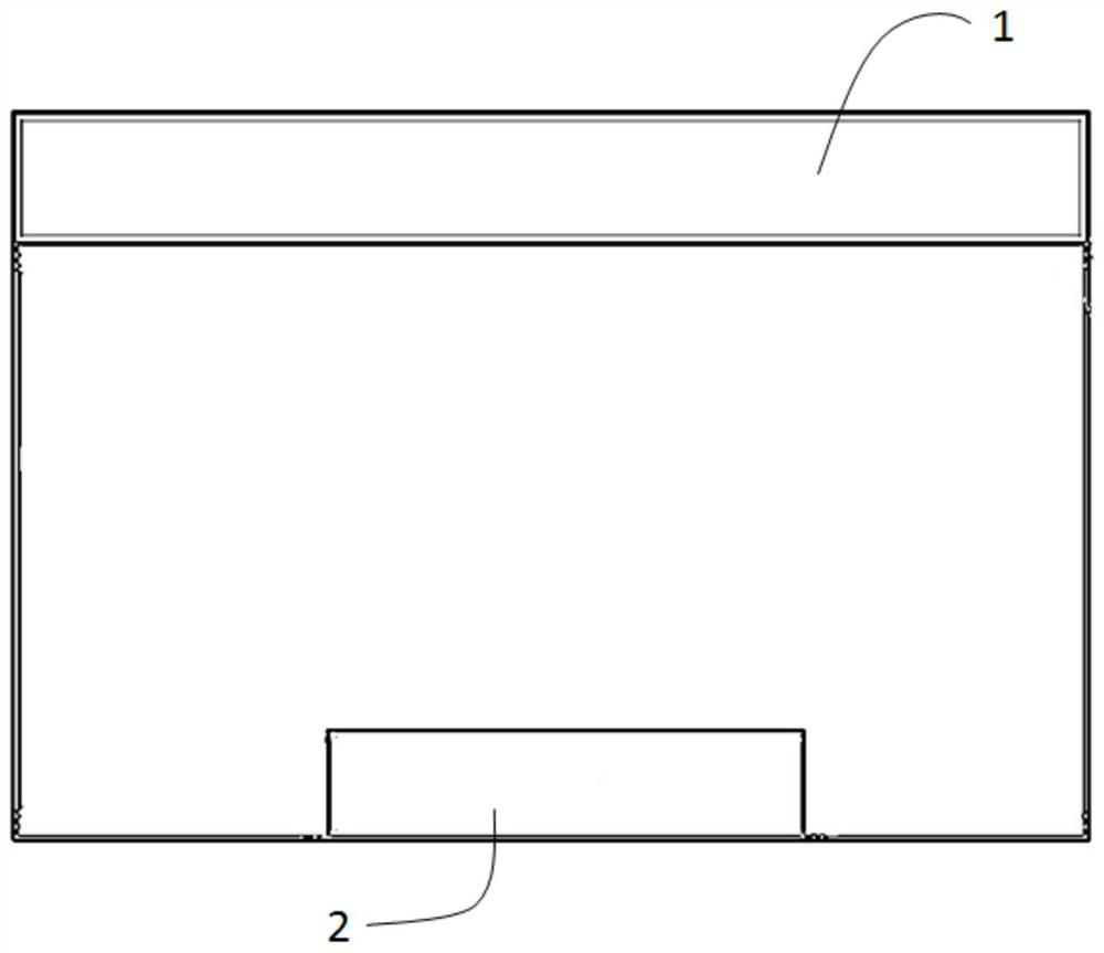
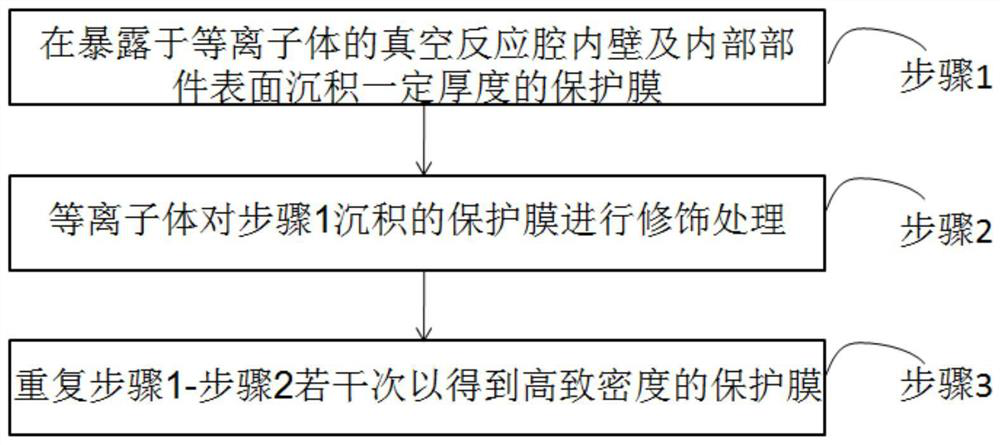
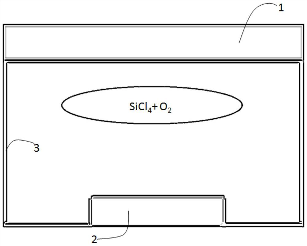

Image

  • Method for coating film in wafer-free vacuum reaction cavity and wafer processing method
  • Method for coating film in wafer-free vacuum reaction cavity and wafer processing method
  • Method for coating film in wafer-free vacuum reaction cavity and wafer processing method

Examples


Embodiment Construction

[0031] The specific implementation manner of the present invention will be described in more detail below with reference to schematic diagrams. Advantages and features of the present invention will be apparent from the following description and claims. It should be noted that all the drawings are in a very simplified form and use imprecise scales, and are only used to facilitate and clearly assist the purpose of illustrating the embodiments of the present invention.

[0032] In the interest of clarity, not all features of an actual embodiment are described. In the following description, well-known functions and constructions are not described in detail since they would obscure the invention with unnecessary detail. It should be appreciated that in the development of any actual embodiment, numerous implementation details must be worked out to achieve the developer's specific goals, such as changing from one embodiment to another in accordance with system-related or business-re...


PUM


Abstract

The invention discloses a method for coating a film in a wafer-free vacuum reaction chamber and a wafer processing method, and the coating method comprises the following steps: 1, conveying a deposition gas into the wafer-free vacuum reaction chamber, and igniting a plasma, depositing a protective film with a certain thickness on the inner wall of the vacuum reaction cavity exposed to the plasma and the surface of an internal part; 2, conveying etching gas into the wafer-free vacuum reaction cavity, igniting the plasma, and allowing the plasma to modify the protective film deposited in the step 1; and 3, repeating the step 1 and the step 2 for a plurality of times to obtain a high-density protective film. The compact protective film is formed on the inner surface of the vacuum reaction cavity in a repeated deposition etching mode, so that the size and the number of particles on the surface of a wafer are reduced, the process is simple, and the implementation is easy.

Description

technical field [0001] The invention relates to a semiconductor manufacturing process, in particular to a film coating method in a vacuum reaction chamber without wafers and a wafer processing method. Background technique [0002] When the plasma in the vacuum reaction chamber reacts with the wafer, polymer deposition will occur on the inner wall of the vacuum reaction chamber and the surface of its components, resulting in sediment and contaminating the wafer. [0003] Usually, after the wafer is processed, it will be moved out of the vacuum reaction chamber, and then the waferless automatic cleaning (Waferless Auto Clean, WAC) process will be performed in the vacuum reaction chamber. The inner wall of the vacuum reaction chamber and the surface of other components are etched and cleaned. The purpose of the cleaning step is to reduce the residues (such as polymers) in the vacuum reaction chamber to reduce the chamber memory effect caused by the residues and reduce the defe...

Claims


Application Information

Patent Timeline
Patent Type & Authority Applications(China)
IPC IPC(8): H01J37/32
CPCH01J37/32853H01J37/3288H01J2237/0203H01J2237/022
Inventor 耿振华刘身健刘志强张洁
Owner ADVANCED MICRO FAB EQUIP INC CHINA
Why Eureka
Eureka Blog
Learn More