Vortex light coding all-optical logic gate based on binary phase shift keying, and implementation method thereof

A technology of binary phase shift keying and implementation method, applied in the direction of logic circuits using optoelectronic devices, logic circuits using specific components, logic circuits, etc., which can solve unfavorable cascade design, weak anti-interference ability, and inconsistent output intensity. and other problems, to achieve good anti-interference ability and easy integration.

Inactive Publication Date: 2021-01-15
GUILIN UNIV OF ELECTRONIC TECH
View PDF5 Cites 1 Cited by
  • Summary
  • Abstract
  • Description
  • Claims
  • Application Information

AI Technical Summary

Problems solved by technology

For example, in [Journal of the Optical Society of America B 24.9 (2007): 2517-2520; Quantum Information Processing 18.8 (2019): 256.], the vortex optically encoded all-optical logic gate proposed by Mach-Zehnder interferometer , some large-volume space optical components (such as mirrors, Duff prisms, pentaprisms) are essential components, which is not conducive to the integration of equipment
In order to meet the needs of equipment integration, the paper [Nanomaterials 9.12(2019):1649.] proposes to use the plasmonic nanoantenna with annular groove structure to realize the all-optical logic gate of vortex optical coding, but the logic gate proposed in this paper still has some shortcomings , including: 1. The logic gate cannot realize XOR logic operation; 2. In order to realize different logic gates, it is necessary to change the vortex state and polarization state of the input signal, which is not conducive to the simplification of logic devices; 3. In OR, AND, NOR In NAND logic gates, the output intensity corresponding to the same output logic state under different input logic states is inconsistent, which is not conducive to the cascade design in practical applications; 4. The XNOR logic gate outputs logic states between "1" and "0". The intensity contrast ratio is only 2:1, and the anti-interference ability is weak

Method used


Image

  • Vortex light coding all-optical logic gate based on binary phase shift keying, and implementation method thereof
  • Vortex light coding all-optical logic gate based on binary phase shift keying, and implementation method thereof
  • Vortex light coding all-optical logic gate based on binary phase shift keying, and implementation method thereof

Examples


Embodiment 1

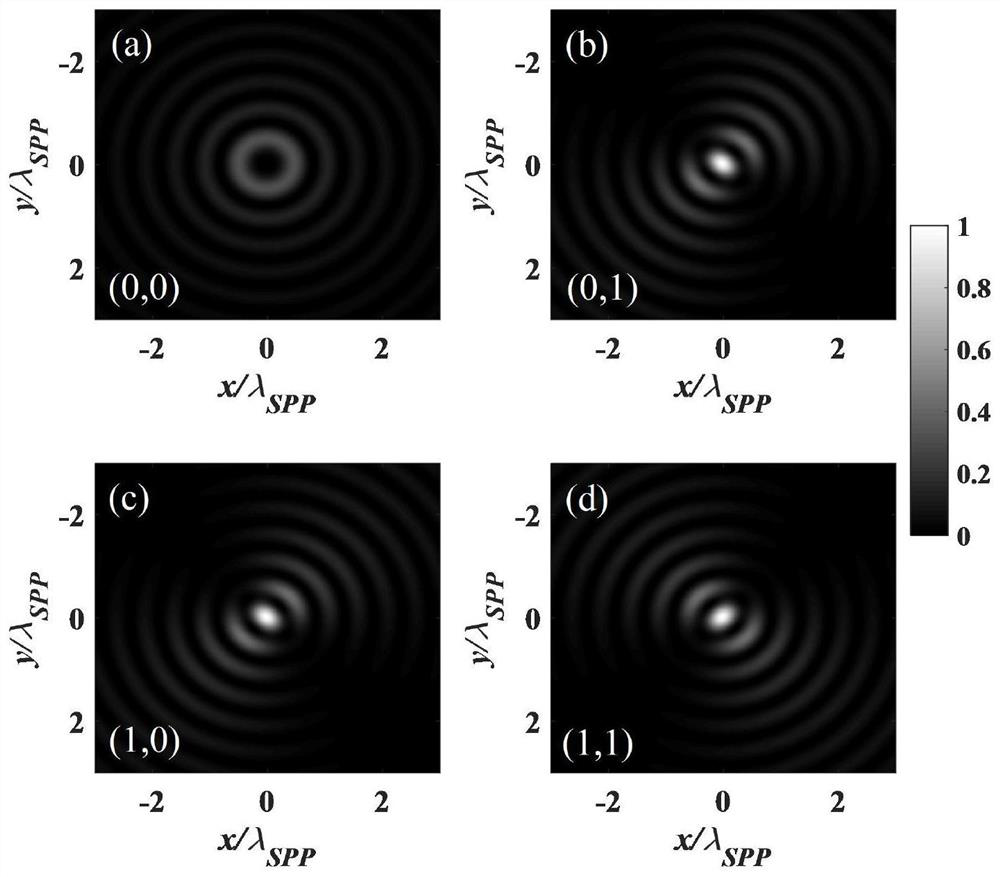
[0028] Embodiment 1: OR logic gate.

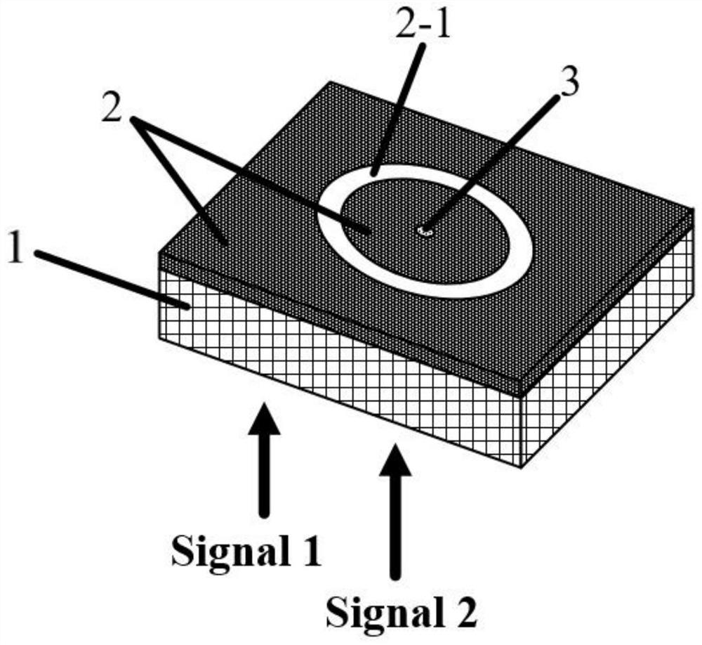
[0029] Such as figure 1 As shown, the vortex optically encoded OR gate in this embodiment includes input signals Signal 1 and Signal 2 , a substrate 1 , a nanometal film 2 , an annular nanogroove 2 - 1 and an output port 3 . The vortex light is vertically incident on the lower surface of the substrate 1, and excites the SPPs at the annular nano-groove 2-1 on the nano-metal film 2. The SPPs transport along the surface of the nanometal film 2 and converge at the output port 3 . Different intensity values ​​of SPPs at the output port 3 are respectively defined as different output logic states. For an ideal OR gate, when the input logic state (A, B) is (0, 0), the SPPs intensity at the output port 3 needs to be 0 to represent the output logic state "0"; when the input logic state (A, B) When (0, 1), (1, 0) and (1, 1), the intensity of SPPs at the output port 3 should be a uniform non-zero value to represent the output logic state "1". Sinc...

Embodiment 2

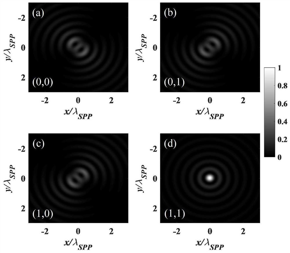
[0030] Embodiment 2: AND logic gate.

[0031] Such as figure 1 As shown, the AND gate of the vortex optical encoding in this embodiment includes input signals Signal 1 and Signal 2 , a substrate 1 , a nanometal film 2 , an annular nanogroove 2 - 1 and an output port 3 . The vortex light is vertically incident on the lower surface of the substrate 1, and excites the SPPs at the annular nano-groove 2-1 on the nano-metal film 2. The SPPs transport along the surface of the nanometal film 2 and converge at the output port 3 . Different intensity values ​​of SPPs at the output port 3 are respectively defined as different output logic states. For an ideal AND gate, when the input logic states (A,B) are (0, 0), (0, 1) and (1, 0), the intensity of SPPs at the output port 3 is 0, representing the output logic state "0 "; when the input logic state (A, B) is (1, 1), the intensity of SPPs at the output port 3 is a value other than 0, representing the output logic state "1". Since the ...


PUM


Abstract

The invention provides a vortex light coding all-optical logic gate based on binary phase shift keying, and an implementation method thereof. The vortex light coding all-optical logic gate structure based on binary phase shift keying comprises a substrate 1, a nanometer metal film 2, an annular nanometer groove 2-1 and an output port 3. The output port 3 is positioned in the center of the annularnanometer groove 2-1. According to the specific implementation method, two beams of orthogonal vortex light are input from the lower surface of a substrate 1 to serve as input signals, and 1 and 0 ofan input logic state are defined by regulating and controlling the phase shift of the input signals. Vortex light excites surface plasmas (SPPS) in the annular nanometer groove 2-1, and the SPPs are transmitted along the surface of the nanometer metal film 2 and converged at the output port 3. Different SPPs intensity values at the output port 3 are respectively defined as different output logic states. Seven basic logic gate functions can be realized on a single structure by adjusting the relative phase difference of the input signals.

Description

[0001] (1) Technical field [0002] The invention relates to the fields of all-optical computing and all-optical information processing, and is especially suitable for manufacturing highly integrated all-optical logic devices. [0003] (2) Background technology [0004] In the era of big data, only the realization of ultra-high-speed network data exchange and information processing can match the demand of large-capacity data transmission. However, traditional electrical information processing equipment has reached a speed bottleneck due to the limitation of electrical response time. All-optical information processing is an effective method to solve this bottleneck problem and is considered to be a strong candidate for the next generation of information processing technology. All-optical logic gates are the key components to realize all-optical information processing, so they are the frontier hotspots of extensive research in recent years [Journal of optics 47.3(2018): 365-376.]...

Claims


Application Information

Patent Timeline
Patent Type & Authority Applications(China)
IPC IPC(8): G02F3/00
CPCG02F3/00
Inventor 刘厚权权志强解正浩苑立波
Owner GUILIN UNIV OF ELECTRONIC TECH
Why Eureka
Try Eureka