Optical communication semiconductor laser and aluminum-containing quantum well active layer butt joint growth method thereof

A quantum well active layer and growth method technology, which is applied in the field of optical communication semiconductor lasers, can solve problems such as reducing docking coupling efficiency, growing voids, increasing process complexity, etc., to avoid oxidation problems, improve performance, and improve docking coupling growth quality effect

Inactive Publication Date: 2021-01-12
武汉云岭光电股份有限公司
View PDF4 Cites 0 Cited by
  • Summary
  • Abstract
  • Description
  • Claims
  • Application Information

AI Technical Summary

Problems solved by technology

[0003] 1. Multi-active layer stacking method, divided into upper laser active layer and lower modulator active layer, the laser active layer in the modulator area is removed, and in the transition area from the laser to the modulator, the upper laser active layer gradually decreases, the light field in the active layer of the laser is gradually transferred to the active layer of the lower modulator. This design epitaxy is relatively simple and simplifies the manufacturing process, but the addition of the active layer of the lower modulator will degrade the performance of the laser;
[0004] 2. Select the epitaxial growth method. Generally, material growth is performed on a masked substrate with two parallel SiO2 strips. The growth rate in the gap between the strips is higher than that in the flat area covered by no mask. , so that epitaxial materials with different thicknesses and compositions are formed in the gap region and the plane region to obtain different light-emitting wavelengths. This method is a gradual transition between the gap region and the plane region, and the optical coupling efficiency is high, but the light-emitting wavelength in this region is also gradual and modulated. The emission wavelength of the laser and the laser region cannot be completely independently optimized;
In this method, the emission wavelengths of the modulator and laser regions can be completely independently optimized, but the growth process of the docking interface is complex, especially for the docking growth of aluminum-containing materials, there is a problem of oxidation of the aluminum material, which leads to growth voids and other problems, which will reduce the docking coupling efficiency.
For this reason, it is generally necessary to perform in-situ etching in the reaction chamber before growth, and then grow after removing the oxide layer, which further increases the complexity of the process.

Method used


Image

  • Optical communication semiconductor laser and aluminum-containing quantum well active layer butt joint growth method thereof
  • Optical communication semiconductor laser and aluminum-containing quantum well active layer butt joint growth method thereof
  • Optical communication semiconductor laser and aluminum-containing quantum well active layer butt joint growth method thereof

Examples


Embodiment 1

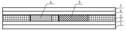
[0038] Such as Figure 1 to Figure 4 , an embodiment of the present invention provides a method for butt growth of an active layer containing an aluminum quantum well in an optical communication semiconductor laser, comprising the following steps:

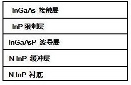
[0039] S1) An N-type InP buffer layer 2 is grown on an N-type InP substrate 1, and then an InGaAsP aluminum-free passive waveguide layer 3, an InP confinement layer, and an InGaAs contact layer are sequentially grown on the N-type InP buffer layer to complete the first epitaxy , to obtain an epitaxial wafer with a structure such as figure 2 shown. In this embodiment, the thickness of the N-type InP buffer layer is 100-500 nm. The InGaAsP aluminum-free passive waveguide layer has a wavelength of 1.05um-1.4um and a thickness of 0.05-0.6um. The thickness of the InP confinement layer is 0.01-0.5um. The thickness of the InGaAs contact layer is 0.01-0.5um.

[0040] S2) Use the PECVD method to grow a SiO2 layer with a thickness of 0.0...

Embodiment 2

[0049] Such as Figure 1 to Figure 4 , this embodiment discloses an optical communication semiconductor laser, comprising a substrate, on which an aluminum-free passive waveguide layer and at least two aluminum-containing quantum well active layers are arranged side by side in the same horizontal plane, and each aluminum-containing quantum well has The source layers are butt-coupled with each other through the aluminum-free passive waveguide layer.

[0050] Further, a buffer layer is provided on the substrate, an aluminum-free passive waveguide layer and at least two aluminum-containing quantum well active layers are arranged on the buffer layer, and the aluminum-free passive waveguide layer and at least two aluminum-containing quantum well active layers are arranged on the buffer layer. An InP confinement layer and a contact layer are arranged on the layer, and the contact layer is located above the InP confinement layer.

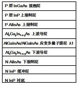
[0051] Further, the aluminum-containing quantum wel...


PUM

PropertyMeasurementUnit
thicknessaaaaaaaaaa

Abstract

The invention relates to an optical communication semiconductor laser and an aluminum-containing quantum well active layer butt joint growth method thereof. The method comprises the following steps: growing an aluminum-free passive waveguide layer on a substrate to complete first epitaxy; removing the aluminum-free passive waveguide layer in a first aluminum-containing quantum well active layer area preset on the primary epitaxial wafer, performing secondary epitaxy, and growing a first aluminum-containing quantum well active layer; and continuously removing the aluminum-free passive waveguidelayer in a preset second aluminum-containing quantum well active layer region on the secondary epitaxial wafer, performing third epitaxy, and growing a second aluminum-containing quantum well activelayer, the aluminum-free passive waveguide layer being spaced between the first aluminum-containing quantum well active layer and the second aluminum-containing quantum well active layer. The epitaxial growth of the aluminum-containing quantum well active layer is carried out on the aluminum-free passive waveguide layer, so that the problem of oxidation of an aluminum-containing material is avoided, and the butt coupling growth quality is improved. And meanwhile, the active layer is made of a high-performance aluminum-containing material, so that the performance of the component can be improved.

Description

technical field [0001] The invention belongs to the technical field of optical communication semiconductor lasers, in particular to an optical communication semiconductor laser and a method for butt joint growth of an active layer containing aluminum quantum wells. Background technique [0002] Different components in optoelectronic integrated chips generally need to use active layers with different light-emitting wavelengths. For this reason, technologies such as multi-active layer stacking, selective epitaxial growth, and active layer butt growth are generally used to modulate integrated lasers with typical electroabsorption (EML ) as an example, the advantages and disadvantages of multiple active layer stacking, selective epitaxial growth, active layer butt growth and other technologies are analyzed in detail: [0003] 1. Multi-active layer stacking method, divided into upper laser active layer and lower modulator active layer, the laser active layer in the modulator area...

Claims


Application Information

Patent Timeline
Patent Type & Authority Applications(China)
IPC IPC(8): H01S5/343
CPCH01S5/34313
Inventor 陈志标
Owner 武汉云岭光电股份有限公司
Why Eureka
Try Eureka