Light-emitting diode epitaxial wafer and preparation method thereof

A technology of light-emitting diodes and epitaxial wafers, which is applied to electrical components, circuits, semiconductor devices, etc., and can solve the problems of non-radiative recombination of electrons and holes, affecting the luminous efficiency of light-emitting diode epitaxial wafers, and many defects

Active Publication Date: 2021-01-05
HC SEMITEK SUZHOU
View PDF8 Cites 0 Cited by
  • Summary
  • Abstract
  • Description
  • Claims
  • Application Information

AI Technical Summary

Problems solved by technology

However, n-type impurity doping is more, which itself will lead to more defects in the GaN layer, and the defects in the n-type GaN layer are easy to extend and move to the active layer, resulting in more defects in the active layer, and the active layer There are more defects in the layer, and it is easy to cause non-radiative recombination of electrons and holes in the defects, which affects the luminous efficiency of the final light-emitting diode epitaxial wafer

Method used


Image

  • Light-emitting diode epitaxial wafer and preparation method thereof
  • Light-emitting diode epitaxial wafer and preparation method thereof
  • Light-emitting diode epitaxial wafer and preparation method thereof

Examples


Embodiment Construction

[0028] In order to make the purpose, technical solution and advantages of the present disclosure clearer, the implementation manners of the present disclosure will be further described in detail below in conjunction with the accompanying drawings.

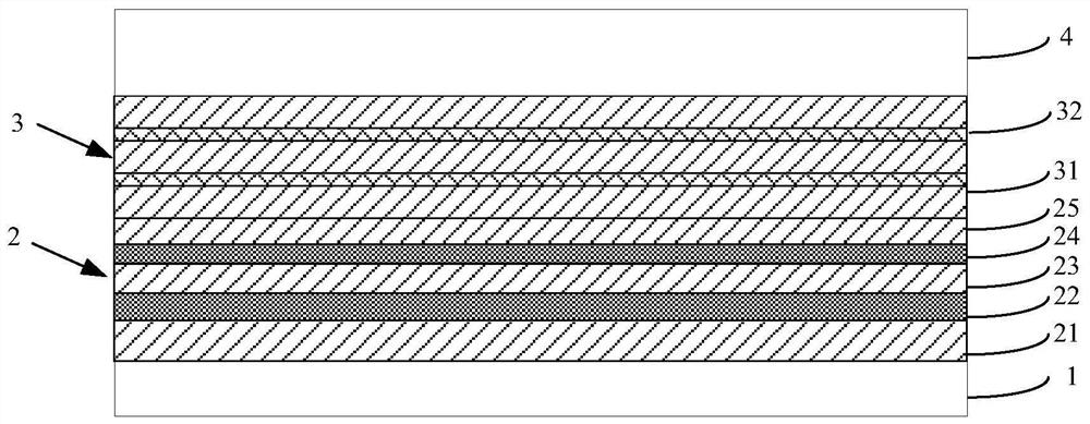
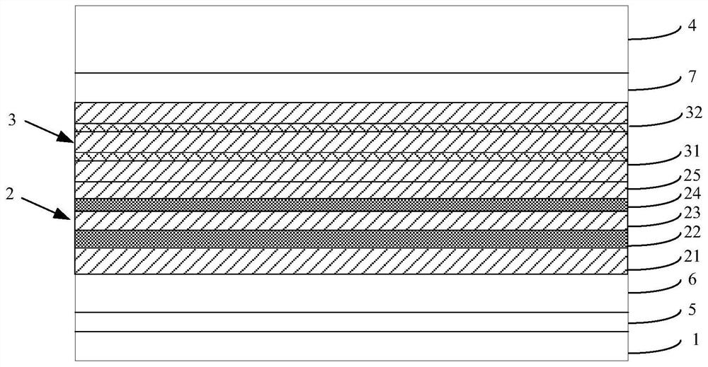
[0029] figure 1 It is a schematic structural diagram of a light emitting diode epitaxial wafer provided by an embodiment of the present disclosure. refer to figure 1 It can be seen that the embodiment of the present disclosure provides a light emitting diode epitaxial wafer, the light emitting diode epitaxial wafer includes a substrate 1 and an n-type layer 2 , an active layer 3 and a p-type GaN layer 4 sequentially stacked on the substrate 1 .

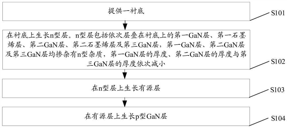
[0030] The n-type layer 2 includes a first GaN layer 21, a first graphene layer 22, a second GaN layer 23, a second graphene layer 24, and a third GaN layer 25 stacked on the substrate 1 in sequence. The first GaN layer 21 , the second GaN layer 23 and the third GaN layer 25 are both dop...


PUM

PropertyMeasurementUnit
Thicknessaaaaaaaaaa
Thicknessaaaaaaaaaa

Abstract

The invention provides a light-emitting diode epitaxial wafer and a preparation method thereof, and belongs to the technical field of light emitting diodes. A first GaN layer, a second GaN layer and athird GaN layer are doped with n-type impurities and are used for providing electrons for compounding. Electrons also have a relatively high migration rate in the first graphene layer and the secondgraphene layer. The migration rate of electrons is increased, and the rate of electrons entering the active layer is increased, so that the concentration of n-type impurities in the n-type layer can be reduced to 6E17-5E18 / cm<-3>. The electron migration rate is accelerated, the reduction of the total electron quantity caused by the reduction of n-type impurities in the first GaN layer, the secondGaN layer and the third GaN layer is compensated, and the luminous efficiency of the light-emitting diode is not influenced. The reduction of the n-type impurities enables the crystal quality of the first GaN layer, the second GaN layer and the third GaN layer to be improved, and finally the light-emitting efficiency of the active layer is effectively improved.

Description

technical field [0001] The present disclosure relates to the technical field of light emitting diodes, in particular to a light emitting diode epitaxial wafer and a preparation method thereof. Background technique [0002] Light-emitting diodes are widely used light-emitting devices, often used in traffic lights, car interior and exterior lights, urban lighting and landscape lighting, etc., and light-emitting diode epitaxial wafers are the basic structure used to prepare light-emitting diodes. A light-emitting diode epitaxial wafer usually includes a substrate and an epitaxial layer grown on the substrate. The epitaxial layer at least includes a GaN buffer layer, an n-type GaN layer, an active layer and a p-type GaN layer stacked on the substrate in sequence. [0003] In the related art, the n-type GaN layer in the light-emitting diode epitaxial wafer is a semiconductor material used to provide electrons, and in order to provide sufficient electrons for the n-type GaN layer,...

Claims


Application Information

Patent Timeline
IPC IPC(8): H01L33/14H01L33/26H01L33/00
CPCH01L33/005H01L33/007H01L33/14H01L33/26
Inventor 姚振从颖董彬忠李鹏
Owner HC SEMITEK SUZHOU
Why Eureka
Try Eureka