Image sensor and control method for the same
An image sensor and control circuit technology, applied in image communication, electric solid-state devices, semiconductor devices, etc., can solve the problems of increasing the number of photodiodes in redundant areas, reducing space utilization, etc., to improve shutter efficiency, eliminate noise, improve The effect of the signal-to-noise ratio
- Summary
- Abstract
- Description
- Claims
- Application Information
AI Technical Summary
Problems solved by technology
Method used
Image


Examples
no. 1 example
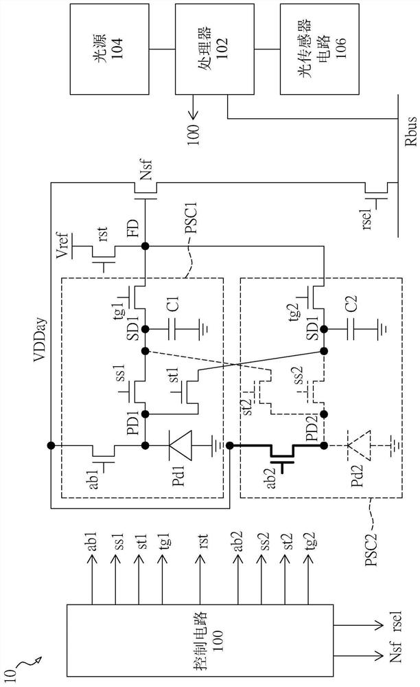
[0038] refer to figure 1 , The first embodiment of the present disclosure provides an image sensor 1 , which includes a pair of pixel sharing circuits PSC1 and PSC2 , a second reset transistor rst, an amplifying transistor Nsf, a readout transistor rsel and a control circuit 100 .
[0039] The pair of pixel sharing circuits PSC1 and PSC2 are connected to the floating diffusion node FD. The pixel sharing circuit PSC1 includes a photonic device Pd1, a first reset transistor ab1, a capturing transistor ss1, a holding transistor tg1, a capacitor C1 and a sharing transistor st1.
[0040] The photonic device Pd1 is configured to receive light energy and generate corresponding charges. The photonic device Pd1 may be a photodiode, which is a semiconductor device that converts light into electric current. When photons are absorbed in the photodiode, a current is generated. A photodiode may include multiple filters and multiple built-in lenses. The first reset transistor ab1 is coup...
no. 2 example
[0056] refer to image 3 , which is a circuit layout diagram of an image sensor according to a second embodiment of the present disclosure.
[0057] In the second embodiment, the control circuit 100 is configured to operate in a first mode, and in the first mode, the control circuit 100 is configured to turn on the first reset transistor ab2, capture transistor ss1, hold The transistor tg1 and the sharing transistor st1 are turned off, and the first reset transistor ab2, the capture transistor ss2 and the sharing transistor st2 of the pixel sharing circuit PSC2 are turned off.
[0058]Specifically, when the ambient light is strong or the light source performs detection and switching operations, the photonic device Pd2 is disabled, the first reset transistor ab2 is turned on to reset the first node PD2, and the capture transistor ss2 and the shared transistor st2 are turned off, Therefore, charges cannot flow into the second nodes SD1 and SD2 as storage points. Therefore, the...
no. 3 example
[0066] refer to Figure 5 , which is a circuit layout diagram of an image sensor according to a third embodiment of the present disclosure.
[0067] In some embodiments, the control circuit 100 operates in the second mode, and in the second mode, the control circuit 100 is configured to turn on capture transistors ss1 and ss2 and hold transistors tg1 and tg2 of a pair of pixel sharing circuits PSC1 and PSC2, And turn off the sharing transistors st1 and st2 of the pair of pixel sharing circuits PSC1 and PSC2.
[0068] Specifically, when the ambient light is weak or the light source is working normally without switching, the photonic devices Pd1 and Pd2 are enabled respectively, and the shared transistors st1 and st2 are turned off to isolate the second nodes SD1 and SD2. Therefore, all photonic devices in the image sensor 10 can be used for sensing, and space utilization efficiency can be improved accordingly.
[0069] The third embodiment provides further steps for the contr...
PUM
 Abstract
Description
Claims
Application Information
 - R&D
- Intellectual Property
- Life Sciences
- Materials
- Tech Scout
- Unparalleled Data Quality
- Higher Quality Content
- 60% Fewer Hallucinations
Browse by: Latest US Patents, China's latest patents, Technical Efficacy Thesaurus, Application Domain, Technology Topic, Popular Technical Reports.
© 2025 PatSnap. All rights reserved.Legal|Privacy policy|Modern Slavery Act Transparency Statement|Sitemap|About US| Contact US: help@patsnap.com