
LED illumination light source construction method for product surface defect detection

A technology of LED lighting and construction methods, which is applied in the directions of measuring devices, optical testing of flaws/defects, and material analysis through optical means, and can solve problems affecting the dynamic range and accuracy of CCD sensor scanning sampling and limited installation space of lighting sources, etc. Achieve good diffusion effect, low power consumption and low cost

Active Publication Date: 2020-12-29
江苏善果缘智能科技有限公司
View PDF6 Cites 1 Cited by
  • Summary
  • Abstract
  • Description
  • Claims
  • Application Information

AI Technical Summary

Problems solved by technology

[0006] The purpose of the present invention is to overcome the existing problem that the installation space of the illumination light source is limited during the detection process of product surface defects, which affects the dynamic range and precision of the scanning sampling of the CCD sensor.

Method used


Image

  • LED illumination light source construction method for product surface defect detection
  • LED illumination light source construction method for product surface defect detection

Examples


Embodiment Construction

[0041]The present invention will be further described below in conjunction with the accompanying drawings of the specification.

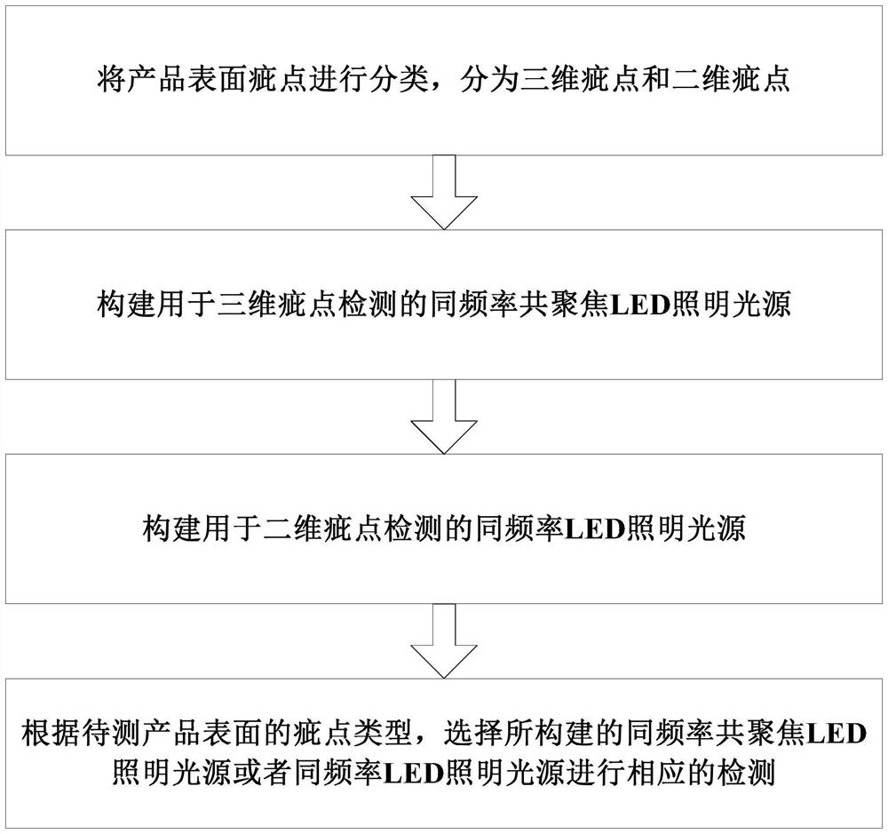
[0042]Such asfigure 1 As shown, the method for constructing an LED lighting source for detecting product surface defects of the present invention includes the following steps:

[0043]Step (A) classify the product surface defects into three-dimensional defects and two-dimensional defects. The three-dimensional defects are those that are inconsistent with the surface of qualified products and are characterized by three-dimensional surface features; the two-dimensional defects are those that are consistent with qualified products. Inconsistent surfaces, defects characterized by two-dimensional surface features, defects characterized by three-dimensional surface features, including protrusions, depressions, etc.; two-dimensional surface defects, including heterogeneous color, stains, damage, etc., among which three-dimensional defects require Parallel light source...


PUM


Abstract

The invention discloses an LED illumination light source construction method for product surface defect detection. The method comprises the steps that product surface defects are classified into three-dimensional defects and two-dimensional defects; a same-frequency confocal LED illumination light source for three-dimensional defect detection is constructed; a same-frequency LED illumination lightsource for two-dimensional defect detection is constructed; and according to the defect type of the surface of a to-be-detected product, the constructed same-frequency confocal LED illumination lightsource or the constructed same-frequency LED illumination light source is selected for corresponding detection. The multi-dimensional defects are classified, the different LED illumination light sources are selected for detection, LED lamp beads can be instantly lightened, overloading can be achieved, brightness is remarkably improved, the heating amount is small, an active heat dissipation component is not needed any more, the overall size is small, field installation of the illumination light sources needed for product surface detection is facilitated, the method is suitable for various industrial environments, more accurate sampling data can be obtained, the dynamic range is wider, and the method adapts to more sample types.

Description

Technical field[0001]The invention relates to the technical field of product surface detection, in particular to a method for constructing an LED lighting source for product surface defect detection.Background technique[0002]The CCD sensor is made of a high-sensitivity semiconductor material, which can convert light into electric charge, which is converted into a digital signal by an analog-to-digital converter for computer processing. At present, CCD sensors are widely used in the detection of surface defects of industrial products. Especially for the detection of various defects on the product surface.[0003]In the detection process of product surface defects (with high accuracy requirements), the sampling environment is very important, and reliable and high-precision data must be provided for the subsequent image processing process to obtain accurate defect detection results.[0004]At present, during the scanning and sampling process of the CCD sensor, the brightness and stability ...

Claims


Application Information

Patent Timeline
Patent Type & Authority Applications(China)
IPC IPC(8): G01N21/88
CPCG01N21/8806G01N2021/8835G01N2021/8838G01N2201/062G01N2201/105
Inventor 周维郑步笑徐存辉陈立新
Owner 江苏善果缘智能科技有限公司
Learn More