Photoelectric high-power microwave amplification method based on wide-band-gap semiconductor device

A high-power microwave and semiconductor technology, applied in the direction of push-pull amplifiers, phase splitters, etc., can solve the problems of low amplification efficiency and low output power, and achieve the effects of high microwave output power, simple structure, and high operating voltage of devices

Active Publication Date: 2020-12-22
NAT UNIV OF DEFENSE TECH
View PDF2 Cites 0 Cited by
  • Summary
  • Abstract
  • Description
  • Claims
  • Application Information

AI Technical Summary

Problems solved by technology

[0009] The technical problem to be solved by the present invention is to propose a photoelectric high-power microwave amplification method based on wide bandgap semiconductor devices to solve the problems of low output power and low amplification efficiency in the technical solution of using semiconductor devices to generate microwaves , can optimize the circuit structure, effectively reduce the electric power loss, and realize the high output power and high efficiency of the photoelectric microwave amplifier

Method used


Image

  • Photoelectric high-power microwave amplification method based on wide-band-gap semiconductor device
  • Photoelectric high-power microwave amplification method based on wide-band-gap semiconductor device
  • Photoelectric high-power microwave amplification method based on wide-band-gap semiconductor device

Examples


Embodiment Construction

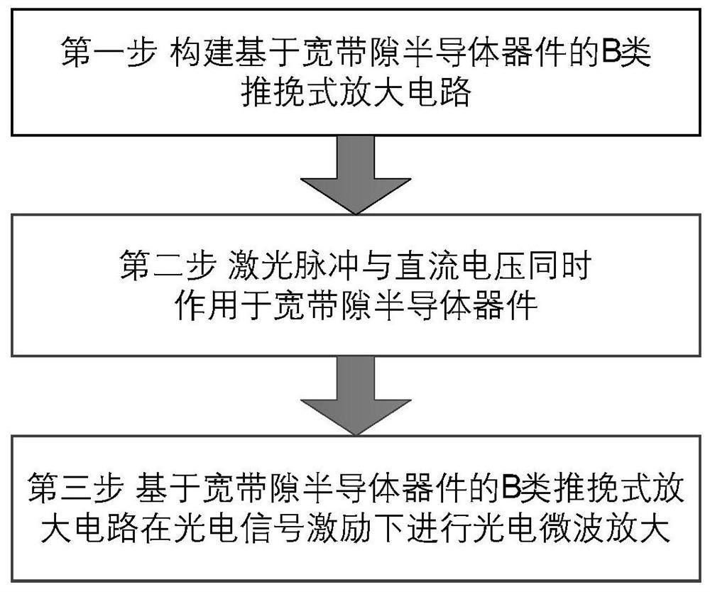
[0045] Such as figure 2 Shown, the present invention comprises the following steps:

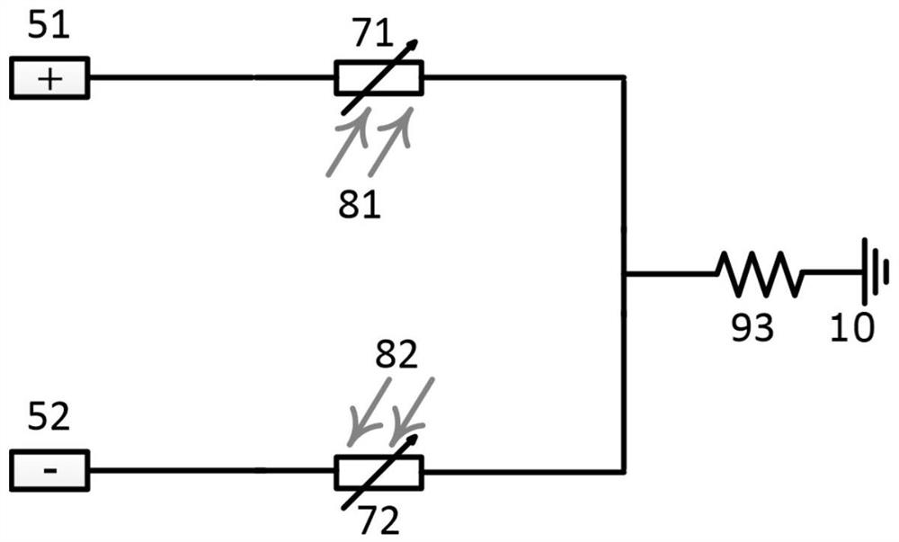
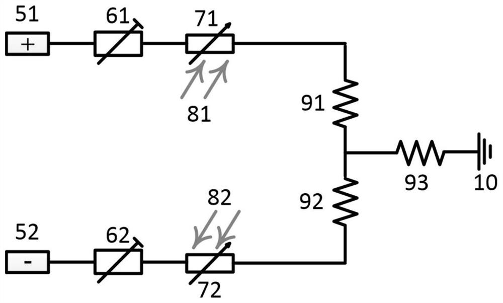
[0046] The first step is to construct a class B push-pull amplifier circuit based on a wide bandgap semiconductor device. The class B push-pull amplifier circuit based on a wide bandgap semiconductor device is as follows: image 3 As shown, there are two power supplies (i.e. the first power supply 51 and the second power supply 52), two pulse forming devices (i.e. the first pulse forming device 61 and the second pulse forming device 62), two wide bandgap semiconductor devices (i.e. The first wide bandgap semiconductor device 71 and the second wide bandgap semiconductor device 72), two current limiting resistors, a load resistor and a ground terminal.

[0047] The first power supply 51 is connected with the first pulse forming device 61 by a high voltage wire, and the first pulse forming device 61 is connected with the wide 71 anode end of the first wide bandgap semiconductor device by a hig...


PUM

PropertyMeasurementUnit
thicknessaaaaaaaaaa
lengthaaaaaaaaaa
diameteraaaaaaaaaa

Abstract

The invention discloses a photoelectric high-power microwave amplification method based on a wide-band-gap semiconductor device, and aims to solve the problems of low output power and low amplification efficiency of an existing amplification circuit. According to the technical scheme, firstly, a B-type push-pull amplification circuit based on a wide-band-gap semiconductor device is constructed, wherein the B-type push-pull amplification circuit is composed of two power supplies, two pulse forming devices, two wide-band-gap semiconductor devices, two current-limiting resistors, a load resistorand a grounding end; the two paths of laser pulses and the voltage generated by the two direct-current power supplies act on two wide-band gap semiconductor devices in the amplifying circuit at the same time; the two wide-band-gap semiconductor devices work as light-operated variable resistors under the excitation of photoelectric signals, and the on-resistance of the two wide-band-gap semiconductor devices is linearly changed along with the light intensity of the high-energy pulse cluster laser, so that the output current and the light intensity are changed in a direct proportion, and photoelectric microwaves are amplified. The amplifying circuit is simple in structure, high in working voltage and high in microwave output power, the unipolar limitation is eliminated, and the problem of low output power is effectively solved.

Description

technical field [0001] The invention relates to the technical field of high-power microwaves, in particular to a photoelectric high-power microwave amplification method based on a wide bandgap semiconductor device. Background technique [0002] In order to cope with the increasingly complex electromagnetic environment under the condition of informationization and the continuous emergence of new waveforms and new spectrums, it is urgent to develop new adaptive microwave sources with flexible and adjustable parameters. The traditional method of generating high-power microwaves has been developed for more than 40 years. It mainly adopts the combination of pulse power devices and relativistic electric vacuum devices. Usually, there are problems such as fixed output microwave parameters, single frequency point or difficult adjustment. On the one hand, this is due to the fact that relativistic vacuum devices usually have a narrow operating frequency range and adopt a mechanical st...

Claims


Application Information

Patent Timeline
Patent Type & Authority Applications(China)
IPC IPC(8): H03F3/26
CPCH03F3/26
Inventor 杨汉武赵昱鑫荀涛王朗宁楚旭朱效庆王日品
Owner NAT UNIV OF DEFENSE TECH
Why Eureka
Try Eureka