Magnetoelectric dipole antenna dual-bandimplementation structure
A dipole antenna, dual-band technology, applied in the field of realization structure of magnetoelectric dipole antenna dual-band, can solve the problems of complex antenna structure and feeding network, increasing antenna size and volume, complex feeding network, etc. To achieve the effect of simple implementation process, simple structure, and easy engineering implementation
- Summary
- Abstract
- Description
- Claims
- Application Information
AI Technical Summary
Problems solved by technology
Method used
Image

Examples
Embodiment 1
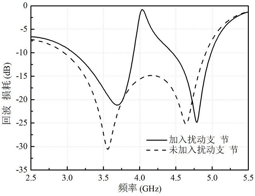
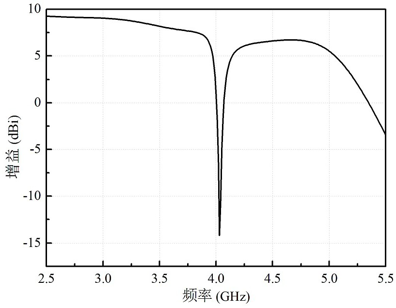
[0028] The implementation structure of the dual frequency band of the magnetoelectric dipole antenna described in the present invention introduces a disturbance branch in the antenna feeder, such as figure 1 shown. 101 is the overall structure of the feeder, 102 is the added disturbance branch, the length D is one quarter of the wavelength in vacuum corresponding to the center frequency of the resulting stopband. The material of 101 is metal with a certain thickness, which can be finished by machining. In the magnetoelectric dipole antenna working in the microwave segment, it needs to be bent and added to the antenna, as shown in 103 .
[0029] Embodiment 1 of the realization structure of the dual frequency band of the magnetoelectric dipole antenna An overall structural diagram of the antenna is as follows figure 2 As shown, it consists of magnetoelectric dipole units 201 and 202 , feeder 203 , and ground plate 204 . Feeder 203 is figure 1 As shown in 103, the ground ...
Embodiment 2
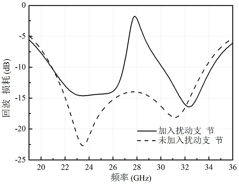
[0034] Embodiment 2 of the realization structure of the dual frequency band of the magnetoelectric dipole antenna The overall structure diagram of the antenna is as follows Figure 5 As shown, it is composed of magnetoelectric dipole units 501, 502, 503 and 504, a feeder 513, a dielectric board 514 and a ground plane 515. The ground plane 515 is the copper-clad bottom surface of the dielectric board. The magnetoelectric dipole units 501, 502, 503 and 504 are located on the upper layer of the dielectric plate 514 and are copper foils, on which L-shaped slots 505, 506, 507 and 508 are respectively etched. 509, 510, 511 and 512 are four groups of metal The via holes are respectively connected to the magnetoelectric dipole of the upper layer and the ground plane of the lower layer. The excitation signal can be connected to the feeder 513 through a hole in the dielectric board 514 through the coaxial cable connector.
[0035] Embodiment 2 of the implementation structure of the dua...
PUM
| Property | Measurement | Unit |
|---|---|---|
| Return loss | aaaaa | aaaaa |
Abstract
Description
Claims
Application Information
 - R&D
- Intellectual Property
- Life Sciences
- Materials
- Tech Scout
- Unparalleled Data Quality
- Higher Quality Content
- 60% Fewer Hallucinations
Browse by: Latest US Patents, China's latest patents, Technical Efficacy Thesaurus, Application Domain, Technology Topic, Popular Technical Reports.
© 2025 PatSnap. All rights reserved.Legal|Privacy policy|Modern Slavery Act Transparency Statement|Sitemap|About US| Contact US: help@patsnap.com