Memory structure and forming method thereof

A memory structure and row-oriented technology, applied in the field of memory, can solve problems such as leakage current and memory performance to be improved, and achieve the effects of increasing area, reducing leakage current, and enhancing control ability

Pending Publication Date: 2020-12-04
CHANGXIN MEMORY TECH INC
View PDF0 Cites 2 Cited by
  • Summary
  • Abstract
  • Description
  • Claims
  • Application Information

AI Technical Summary

Problems solved by technology

[0003] However, the storage structure composed of capacitors and transistors in the existing me...

Method used


Image

  • Memory structure and forming method thereof
  • Memory structure and forming method thereof
  • Memory structure and forming method thereof

Examples


Embodiment Construction

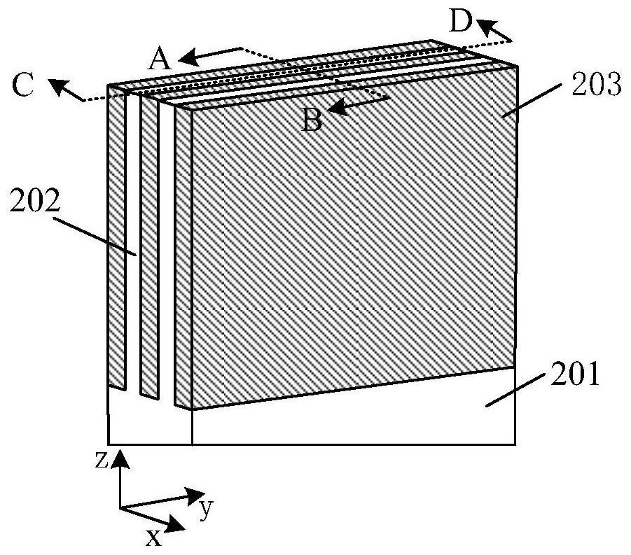
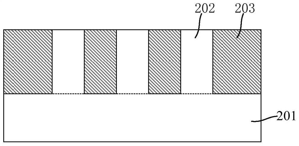
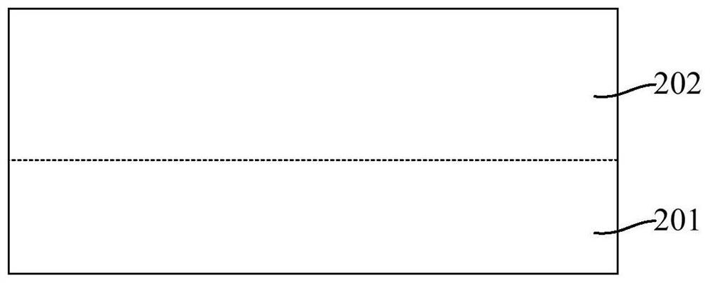
[0044] As mentioned in the background, the existing memory structure has a problem of leakage current, and the performance of the memory still needs to be improved.

[0045] Research has found that in order to reduce the leakage current of the storage capacitor in the DRAM and increase the turn-off resistance of the transistor, a trench-type transistor structure is usually used. The specific structure of the trench-type transistor structure includes a semiconductor substrate; The trench in the bottom, the gate in the trench; the drain and source regions in the semiconductor substrate on both sides of the trench. In the trench type transistor, the gate is connected to the word line, the drain is connected to the bit line, and the source is connected to the capacitor. When the transistor is turned off, some electrons will leak from the source region into the semiconductor substrate, making the storage capacity of the DRAM memory worse. Therefore, how to reduce the leakage curren...


PUM


Abstract

The invention relates to a storage structure and a forming method thereof. The storage structure comprises: a semiconductor substrate, wherein a plurality of discrete active regions arranged in rows and columns are formed on the semiconductor substrate, a first groove is arranged between adjacent active regions, and the first groove is filled with an insulating layer; two second grooves located ineach active region and distributed in the row direction, wherein each active region is divided into a drain electrode located in the middle and two source electrodes located on the two sides of the drain electrode through the two second grooves; third grooves located in part of the insulating layers on the two sides of the bottoms of the second grooves, wherein at least part of the surfaces of the side walls of the two sides of the active region on the bottoms of the second grooves are exposed out of the third grooves, the third grooves are communicated with the corresponding second grooves,and every two adjacent third grooves in the row direction are not communicated; and gate structures positioned in the second grooves and the third grooves. According to the storage structure, the magnitude of leakage current is reduced.

Description

technical field [0001] The invention relates to the field of memory, in particular to a memory structure and a forming method thereof. Background technique [0002] Dynamic Random Access Memory (Dynamic Random Access Memory, DRAM) is a semiconductor storage device commonly used in computers, which consists of many repeated storage units. Each memory cell usually includes a capacitor and a transistor. The gate of the transistor is connected to the word line, the drain is connected to the bit line, and the source is connected to the capacitor. The voltage signal on the word line can control the opening or closing of the transistor, and then through the bit line Read the data information stored in the capacitor, or write the data information into the capacitor through the bit line for storage. [0003] However, the storage structure composed of capacitors and transistors in the existing memory has the problem of leakage current, and the performance of the memory still needs to...

Claims


Application Information

Patent Timeline
IPC IPC(8): H01L27/108H01L21/8242
CPCH10B12/34H10B12/053H10B12/488H01L29/4236
Inventor 不公告发明人
Owner CHANGXIN MEMORY TECH INC
Why Eureka
Try Eureka