Silicon/perovskite laminated solar cell
A technology of solar cells and perovskite cells, applied in the field of solar cells, can solve problems such as low stability, affecting the life of silicon/perovskite solar cells, short-circuit current decline, etc., and achieve good stability
- Summary
- Abstract
- Description
- Claims
- Application Information
AI Technical Summary
Problems solved by technology
Method used
Image


Examples
Embodiment 1
[0074] Example 1: Preparation of silicon / wide bandgap perovskite parallel stack cell
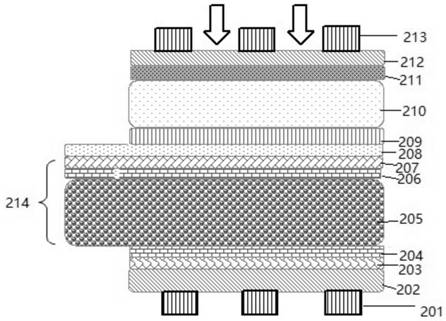
[0075] S1. On the n-type silicon wafer that has been cleaned and textured, each of the two surfaces is coated with an intrinsic amorphous silicon layer with a thickness of 10nm and 12nm by plasma-enhanced chemical vapor deposition; and the thickness of the n-type silicon wafer is A part of one side is reserved as an area for leading out the middle transparent conductive layer;
[0076] S2. Depositing a layer of p-type amorphous silicon with a thickness of 10 nm on the 10 nm thick intrinsic amorphous silicon layer. Depositing a layer of n-type amorphous silicon with a thickness of 15 nm on the 12 nm thick intrinsic amorphous silicon layer;
[0077] S3. Prepare indium tin oxide on the n-type amorphous silicon layer by magnetron sputtering, with a thickness of 100nm, and prepare indium tin oxide on the p-type amorphous silicon layer by magnetron sputtering, with a thickness of 120nm;
[0078]...
Embodiment 2
[0084] Example 2: Preparation of silicon / narrow bandgap perovskite parallel stack cell (p-side light incident)
[0085] S1. On the n-type silicon wafer that has been cleaned and textured, each of the two surfaces is coated with an intrinsic amorphous silicon layer by plasma-enhanced chemical vapor deposition, with a thickness of 10nm and 12nm respectively;
[0086] S2. Depositing a layer of p-type amorphous silicon with a thickness of 10 nm on the 10 nm thick intrinsic amorphous silicon layer. Depositing a layer of n-type amorphous silicon with a thickness of 15 nm on the 12 nm thick intrinsic amorphous silicon layer;
[0087] S3. Prepare indium tin oxide on the n-type amorphous silicon layer by magnetron sputtering, with a thickness of 100nm, and prepare indium tin oxide on the p-type amorphous silicon layer by magnetron sputtering, with a thickness of 120nm;
[0088] S4. Depositing a layer of nickel oxide by electron beam on the indium tin oxide layer of the p-type amorphou...
Embodiment 3
[0093] Example 3: Preparation of silicon / narrow bandgap perovskite parallel stack cell (n-side light incident)
[0094] S1. On the n-type silicon wafer that has been cleaned and textured, each of the two surfaces is coated with an intrinsic amorphous silicon layer by plasma-enhanced chemical vapor deposition, with a thickness of 10nm and 12nm respectively;
[0095] S2. Depositing a layer of p-type amorphous silicon with a thickness of 10 nm on the 10 nm thick intrinsic amorphous silicon layer. Depositing a layer of n-type amorphous silicon with a thickness of 15 nm on the 12 nm thick intrinsic amorphous silicon layer;
[0096] S3. Prepare indium tin oxide on the p-type amorphous silicon layer by magnetron sputtering, with a thickness of 100nm, and prepare indium tin oxide on the n-type amorphous silicon layer by magnetron sputtering, with a thickness of 120nm;
[0097] S4. Depositing a layer of tin oxide by electron beam on the indium tin oxide layer of the n-type amorphous s...
PUM
| Property | Measurement | Unit |
|---|---|---|
| band gap | aaaaa | aaaaa |
| band gap | aaaaa | aaaaa |
| thickness | aaaaa | aaaaa |
Abstract
Description
Claims
Application Information
 - Generate Ideas
- Intellectual Property
- Life Sciences
- Materials
- Tech Scout
- Unparalleled Data Quality
- Higher Quality Content
- 60% Fewer Hallucinations
Browse by: Latest US Patents, China's latest patents, Technical Efficacy Thesaurus, Application Domain, Technology Topic, Popular Technical Reports.
© 2025 PatSnap. All rights reserved.Legal|Privacy policy|Modern Slavery Act Transparency Statement|Sitemap|About US| Contact US: help@patsnap.com