A kind of dynamic frequency selective surface structure and preparation method thereof
A technology of frequency selective surface and dynamic frequency selection, which is applied in the electromagnetic field, can solve problems such as deterioration of the performance of integrated circuit components, and achieve the effects of avoiding overheating of the dielectric substrate and deformation of the unit structure, avoiding energy loss, and avoiding weight increase
- Summary
- Abstract
- Description
- Claims
- Application Information
AI Technical Summary
Problems solved by technology
Method used
Image
Examples
example 1
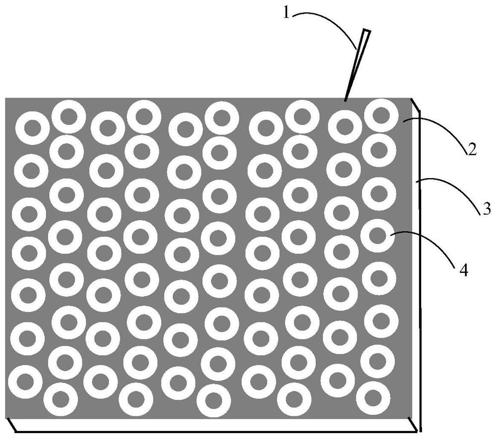
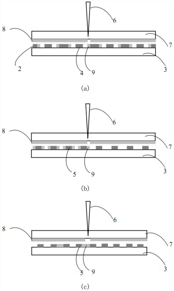
[0059] A sample F4B-2 dielectric substrate with a size of 500mm×500mm, a thickness of 0.5mm, a relative permittivity ε=2.65 and a copper film with a thickness of 0.03mm was selected, and the laser selective etching technology was used on the sample. Selectively remove the copper film material, and prepare a gap ring-shaped unit structure with an outer ring radius of 2.3 mm, an inner ring radius of 1.9 mm, and a period (that is, the distance between the center of the adjacent unit and the center) of 5 mm. A bandpass FSS periodic array with a fixed resonant frequency. Then, using laser-induced forward transfer technology (LIFT), the undoped ionic VO deposited on the lower surface of the glass substrate 2 The film is transferred with high precision to the outer wall of the inner ring of the gap annular unit structure, and is in close contact with the copper film of the inner ring, VO 2 The film has a width of 0.2 mm and a thickness of 0.03 mm, and is prepared into a composite un...
example 2
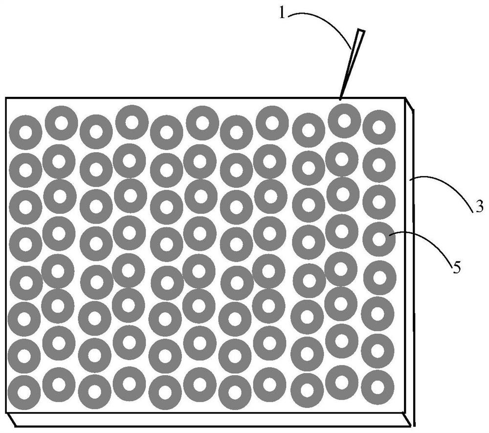
[0061] A sample F4B-2 dielectric substrate with a size of 500mm×500mm, a thickness of 0.5mm, a relative permittivity ε=2.65 and a copper film with a thickness of 0.03mm was selected, and the laser selective etching technology was used on the sample. Selectively remove the copper film material, and prepare a ring-shaped unit structure of copper sheets with an outer ring radius of 2.3 mm, an inner ring radius of 1.9 mm, and a period of 5 mm, forming a band-stop FSS periodic array with a fixed resonant frequency . Then, using laser-induced forward transfer technology (LIFT), the undoped ionic VO deposited on the lower surface of the glass substrate 2 The film is transferred to the outer wall of the inner ring of the ring-shaped unit structure of the copper sheet with high precision, and is in close contact with the copper film of the inner ring, VO 2 The film has a width of 0.3 mm and a thickness of 0.03 mm, and is prepared into a composite unit structure. When the ambient temp...
example 3
[0063] A sample F4B-2 dielectric substrate with a size of 500mm×500mm, a thickness of 0.5mm, a relative permittivity ε=2.65 and a copper film with a thickness of 0.03mm was selected, and the laser selective etching technology was used on the sample. Selectively remove the copper film material, and prepare a slot ring-shaped unit structure with an outer ring radius of 2.3mm, an inner ring radius of 1.9mm, and a period of 5mm, forming a band-pass FSS periodic array with a fixed resonant frequency. Then, laser-induced forward transfer (LIFT) was used to transfer the doped 10% Mo ion VO deposited on the lower surface of the glass substrate. 2 The film (phase transition temperature is 308K) is transferred to the outer wall of the inner ring of the gap annular unit structure with high precision, and is in close contact with the inner ring copper film, doped with Mo ions VO 2 The width of the film is 0.1mm and the thickness is 0.03mm; then the laser-induced forward transfer technolog...
PUM
| Property | Measurement | Unit |
|---|---|---|
| Resonant frequency | aaaaa | aaaaa |
| width | aaaaa | aaaaa |
| thickness | aaaaa | aaaaa |
Abstract
Description
Claims
Application Information
 - R&D
- Intellectual Property
- Life Sciences
- Materials
- Tech Scout
- Unparalleled Data Quality
- Higher Quality Content
- 60% Fewer Hallucinations
Browse by: Latest US Patents, China's latest patents, Technical Efficacy Thesaurus, Application Domain, Technology Topic, Popular Technical Reports.
© 2025 PatSnap. All rights reserved.Legal|Privacy policy|Modern Slavery Act Transparency Statement|Sitemap|About US| Contact US: help@patsnap.com


