Inorganic material film layer, thin film encapsulation layer, display substrate and manufacturing method thereof

An inorganic material, thin film encapsulation technology, used in semiconductor/solid-state device manufacturing, electrical components, electrical solid-state devices, etc., can solve problems such as stress failure, and achieve the effect of slowing down the flow rate

Pending Publication Date: 2020-11-06
BOE TECH GRP CO LTD +1
View PDF3 Cites 1 Cited by
  • Summary
  • Abstract
  • Description
  • Claims
  • Application Information

AI Technical Summary

Problems solved by technology

[0005] However, the current design direction of display devices tends to reduce the thickness of the overall screen. After the display device with the A-Hole project adopts the Baseline structure, due to the limitation of the edge leveling effect, it is necessary to print a thicker film layer when inkjet printing of the organic material film layer To cover possible surface wrinkles (Orange mura), resulting in thicker organic material film thickness after the display device of the A-Hole project adopts the Baseline structure; when the display device of the A-Hole project adopts the Interfical structure, and a larger When the shrinkage value is set, there will be no overflow phenomenon in theory, and the thickness of the organic material film layer can also be reduced, but at a large shrinkage value, the groove (Slot) is not effectively filled by the organic material film layer, and there is a stress failure risk

Method used


Image

  • Inorganic material film layer, thin film encapsulation layer, display substrate and manufacturing method thereof
  • Inorganic material film layer, thin film encapsulation layer, display substrate and manufacturing method thereof

Examples


Embodiment Construction

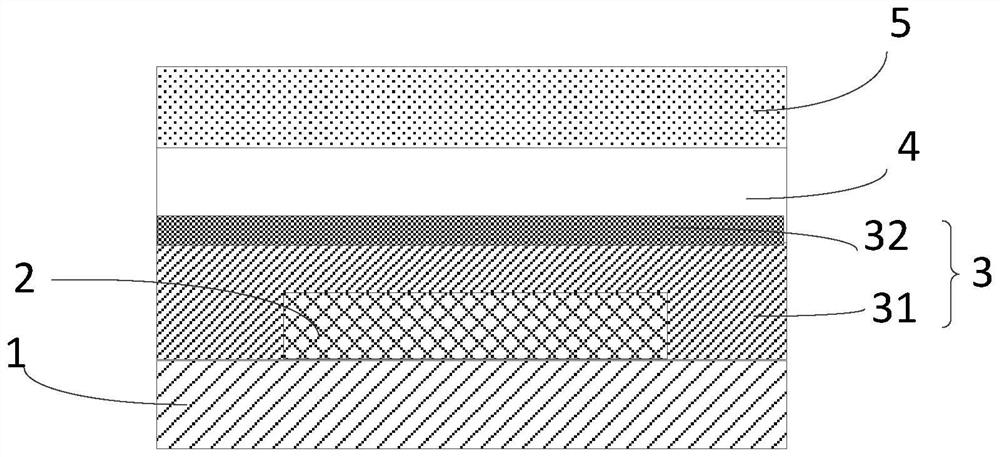
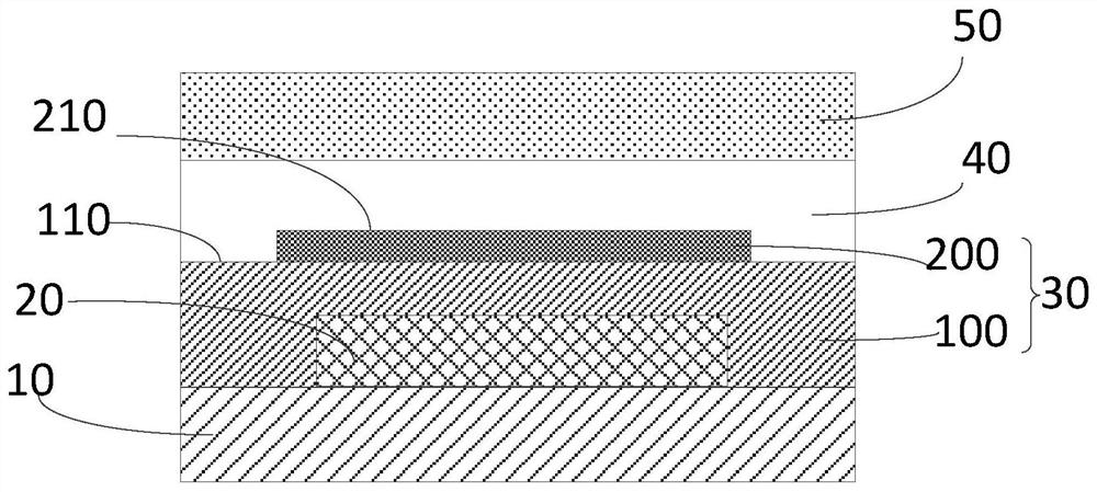
[0043] In order to make the purpose, technical solutions and advantages of the embodiments of the present disclosure clearer, the technical solutions of the embodiments of the present disclosure will be clearly and completely described below in conjunction with the accompanying drawings of the embodiments of the present disclosure. Apparently, the described embodiments are some of the embodiments of the present disclosure, not all of them. All other embodiments obtained by persons of ordinary skill in the art based on the described embodiments of the present disclosure belong to the protection scope of the present disclosure.

[0044] In the description of the present disclosure, it should be noted that the terms "center", "upper", "lower", "left", "right", "vertical", "horizontal", "inner", "outer" etc. The indicated orientation or positional relationship is based on the orientation or positional relationship shown in the drawings, and is only for the convenience of describin...


PUM


Abstract

The present disclosure provides an inorganic material film layer, a thin film encapsulation layer, a display substrate and a manufacturing method thereof, the inorganic material film layer comprising:a first film layer including a first surface; and a second film layer which is formed on the first surface of the first film layer, the second film layer comprises a second surface located on the side away from the first film layer, and the surface tension of the second surface is larger than that of the first surface; the first surface comprises a central area and a peripheral area, the orthographic projection of the second film layer on the first surface is smaller than the area of the first surface, the second film layer covers the central area, and the peripheral area is not covered by the second film layer to form a peripheral exposed area. According to the inorganic material film layer provided by the invention, the organic material film layer can be fully leveled during ink-jet printing, an overflow phenomenon does not occur, the thickness of the film layer is ensured not to be too thick, and the risk of stress failure can be reduced.

Description

technical field [0001] The present disclosure relates to the field of display technology, in particular to an inorganic material film layer, a thin film encapsulation layer, a display substrate and a manufacturing method thereof. Background technique [0002] In the related art, in an OLED (Organic Electroluminesence Display, Organic Light Emitting Diode) display device, in order to prevent the luminescent material from being intruded by water vapor, and to have a longer working life, after the light emitting element is formed on the substrate of the OLED device, it will A thin film encapsulation layer is prepared to protect the luminescent material. [0003] Usually, the thin film encapsulation layer structure is sealed with three layers, which are the first inorganic material film layer, organic material film layer and the second inorganic material film layer. The film layer structure of the first inorganic material film layer can be divided into two types: Baseline struct...

Claims


Application Information

Patent Timeline
IPC IPC(8): H01L51/52H01L51/56H01L27/32
CPCH10K59/00H10K50/84H10K50/8445H10K50/844H10K71/00
Inventor 谈耀宏戴明吴永凯
Owner BOE TECH GRP CO LTD
Why Eureka
Try Eureka