
LED backlight source, LED backlight module and preparation method

A technology of LED backlight and backlight module, which is applied in optics, nonlinear optics, instruments, etc., can solve the problem of large thickness of LED display screen, and achieve the effect of thickness reduction and thickness reduction

Inactive Publication Date: 2020-10-16
HCP TECH CO LTD
View PDF6 Cites 3 Cited by
  • Summary
  • Abstract
  • Description
  • Claims
  • Application Information

AI Technical Summary

Problems solved by technology

[0005] In view of the above-mentioned shortcomings of the prior art, the purpose of the present invention is to provide an LED backlight, LED backlight module and preparation method, which are used to solve the problem of large thickness of the LED display in the prior art

Method used


Image

  • LED backlight source, LED backlight module and preparation method
  • LED backlight source, LED backlight module and preparation method
  • LED backlight source, LED backlight module and preparation method

Examples


Embodiment 1

[0043] Such as Figure 1 to Figure 7 As shown, the present embodiment provides a method for preparing an LED backlight, and the LED backlight can be applied to a liquid crystal display, and the preparation method includes steps:

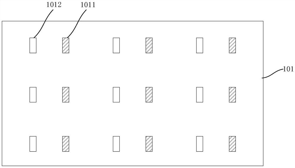
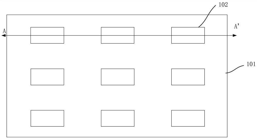
[0044] Such as Figure 1~4 As shown, step 1) is first performed, providing a substrate 101 and LED chip 102, the LED chip 102 has a substrate 1023, and the LED chip 102 is crystal-bonded on the substrate 101 by flip-chip, so that An LED array is formed on the substrate 101 .

[0045] The substrate 101 may be one of a PCB substrate and a glass substrate, and the type of the PCB substrate may be FR4, BT, BT-like, FPC or the like.

[0046] Such as figure 1As shown, the substrate 101 has a thin film transistor array (TFT Array) and an electrode array, the electrode array includes a first electrode 1011 array and a second electrode 1012 array, and the first electrode 1011 array includes a first electrode array arranged in an array electrode 1011, the...

Embodiment 2

[0066] Such as Figure 1 to Figure 9 Shown, the present invention provides a kind of preparation method of LED backlight module, described LED backlight module can be applied to liquid crystal display, and described preparation method comprises:

[0067] Such as Figure 1 to Figure 8 As shown, step 1) is first carried out, and the LED backlight is prepared by the method for preparing the LED backlight as described in Example 1.

[0068] Such as Figure 9 As shown, then proceed to step 2) to fabricate a color conversion layer 203 on the LED backlight.

[0069] The color conversion layer 203 may be one of quantum dot film and phosphor film.

[0070] For example, the color conversion layer 203 is a quantum dot film, and there are quantum dots in the quantum dot film, and the quantum dots emit red light and green light under the excitation of the blue light emitted by the blue LED chip; or, the quantum dots Red light is emitted under the joint excitation of blue light or green ...


PUM

PropertyMeasurementUnit
thicknessaaaaaaaaaa
thicknessaaaaaaaaaa

Abstract

The invention provides an LED backlight source, an LED backlight module and a preparation method. The LED backlight source comprises a substrate; a LED array, wherein a substrate of an LED chip of theLED array is removed, and the LED chip is connected to the base plate in an inverted mode. According to the LED backlight source, the Mini LED array is bonded on the substrate in an inverted manner,the substrate of all Mini LED chips of the Mini LED array is removed, so that the thickness of the liquid crystal display backlight module is greatly reduced, and compared with a traditional liquid crystal display backlight module, the thickness of the liquid crystal display backlight module can be reduced by more than 85 microns. The LED backlight source is suitable for consumer electronics suchas mobile phones and tablet personal computers, and the requirement of the market for lightness and thinness of the LED display screen is met.

Description

technical field [0001] The invention belongs to the field of semiconductor display, and in particular relates to an LED backlight source, an LED backlight module and a preparation method. Background technique [0002] At present, among flat panel display technologies, liquid crystal display technology occupies a mainstream position and is widely used. Large-screen TVs based on liquid crystal display technology have been popularized on a large scale, and the mainstream size has reached 65 inches. At the same time, 98-inch ultra-large LCD TVs have entered the 20,000 yuan range. In the existing liquid crystal display technology, the application penetration rate of LED as a backlight source in the field of liquid crystal panel display has exceeded 90%. [0003] There are mainly two types of backlight module architectures: side-type and direct-type. The side-type LED backlight is to install the LED light source on the side of the light guide plate. Scattering directs the light ...

Claims


Application Information

Patent Timeline
Patent Type & Authority Applications(China)
IPC IPC(8): G02F1/13357H01L25/075H01L33/48H01L33/62
CPCG02F1/133603H01L25/0753H01L33/48H01L33/62H01L2933/0033H01L2933/0066
Inventor 卢敬权庄文荣孙明
Owner HCP TECH CO LTD
Learn More