A detection method for wafer passivation layer defects
A detection method and passivation layer technology, which can be used in optical testing flaws/defects, measurement devices, semiconductor/solid-state device testing/measurement, etc., can solve the problems of missed inspection, structural defects, surface defects, etc. rate, wide application range, wide coverage effect
- Summary
- Abstract
- Description
- Claims
- Application Information
AI Technical Summary
Problems solved by technology
Method used
Image
Examples
Embodiment 1
[0022] The improved wafer passivation layer defect detection method of the present invention can be used for detection of wafers of various sizes, but in this embodiment, the wafer to be tested is a 12-inch product wafer whose top layer metal is copper.
[0023] The steps of the detection method for the defects of the wafer passivation layer in this embodiment are:
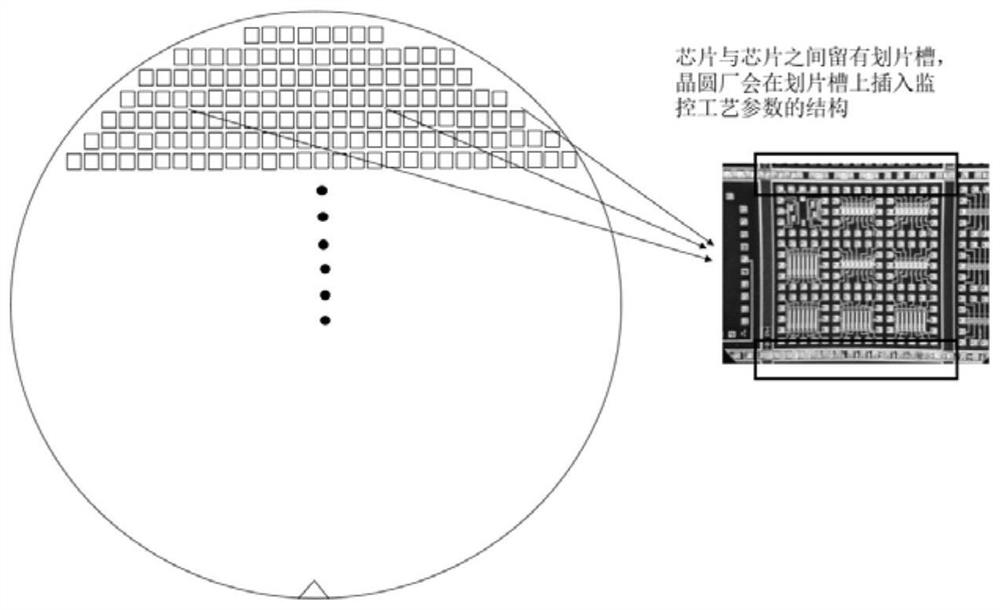
[0024] (1) Provide a 12-inch wafer to be tested that has been inserted into a specific interdigitated structure detection circuit in the dicing groove during the import stage of the design file, and perform a WAT test on these detection circuits to obtain their capacitance and resistance values;
[0025] Such as figure 1 As shown, in order to monitor the stability of the on-line process, a specific test structure will be inserted on the scribe groove between the chips in the wafer. The density of the inserted electrical monitoring structure and the structure of the detection circuit are determined by the requir...
Embodiment 2
[0034] The difference between Embodiment 2 and Embodiment 1 is that the wafer to be tested is a 12-inch product wafer with a different chip circuit structure. The defect rate of the wafer passivation layer of the 12-inch wafer described in this embodiment after being detected by AEI is 0.51%, and the defect rate of the wafer passivation layer obtained through the detection steps of this embodiment is 0.56%, and the detection result is consistent with that of Example 1 Similarly, although the defect rate of the passivation layer of the product wafer in this embodiment is higher and the pass rate is slightly lower, the defect discovery rate of the detection method used in the present invention is still higher than that of the traditional optical AEI detection method.
Embodiment 3
[0036]The difference between embodiment 3 and embodiment 1 is that the wafer to be tested is a 12-inch test control chip wafer whose top metal is copper and the chip circuit structure is different. The defect rate of the wafer passivation layer of the 12-inch wafer described in this embodiment is 3.89% after the AEI detection, and the defect rate of the wafer passivation layer obtained through the detection steps of this embodiment is 4.21%, showing that the passivation layer provided by the present invention has a defect rate of 4.21%. The chemical layer defect detection method can be applied to normal product wafers or control wafers with many defects for detection and testing, and the accuracy and precision are higher than the AEI detection method.
PUM
 Abstract
Description
Claims
Application Information
 - Generate Ideas
- Intellectual Property
- Life Sciences
- Materials
- Tech Scout
- Unparalleled Data Quality
- Higher Quality Content
- 60% Fewer Hallucinations
Browse by: Latest US Patents, China's latest patents, Technical Efficacy Thesaurus, Application Domain, Technology Topic, Popular Technical Reports.
© 2025 PatSnap. All rights reserved.Legal|Privacy policy|Modern Slavery Act Transparency Statement|Sitemap|About US| Contact US: help@patsnap.com


