Tin bonding connection structure of crystal oscillator test base

A connection structure and test seat technology, which is applied to the components of electrical measuring instruments, measuring devices, and measuring electrical variables, etc., can solve problems such as hindering the heat dissipation effect of the device, difficult operation, and easily damaged pads, so as to enhance maintainability , fast replacement, fast heat dissipation effect

Active Publication Date: 2020-09-22
成都恒晶科技有限公司
View PDF11 Cites 0 Cited by
  • Summary
  • Abstract
  • Description
  • Claims
  • Application Information

AI Technical Summary

Problems solved by technology

[0002] As the heart of electronic equipment, the importance of crystal oscillators in equipment is self-evident; with the development of technology, crystal oscillators are gradually chipped and miniaturized, which has higher requirements for the connection structure of test tools. The test seat is installed on the test board by directly welding the test seat pins into the test card installation hole. When the test seat needs to be repaired and replaced in this way, it is necessary to absorb the welded pads one by one, remove the solder, and then The test seat can only be removed, the operation is difficult, the pad is easily damaged, and the soldering tin is arranged in the test card installation hole, which also hinders the heat dissipation effect of the device during use, and there are disadvantages in use. Based on this, the present invention designs a crystal oscillator test tool. The tin connection structure of the seat is used to solve the above problems

Method used


Image

  • Tin bonding connection structure of crystal oscillator test base
  • Tin bonding connection structure of crystal oscillator test base
  • Tin bonding connection structure of crystal oscillator test base

Examples


Embodiment Construction

[0018] The following will clearly and completely describe the technical solutions in the embodiments of the present invention with reference to the accompanying drawings in the embodiments of the present invention. Obviously, the described embodiments are only some, not all, embodiments of the present invention. Based on the embodiments of the present invention, all other embodiments obtained by persons of ordinary skill in the art without creative efforts fall within the protection scope of the present invention.

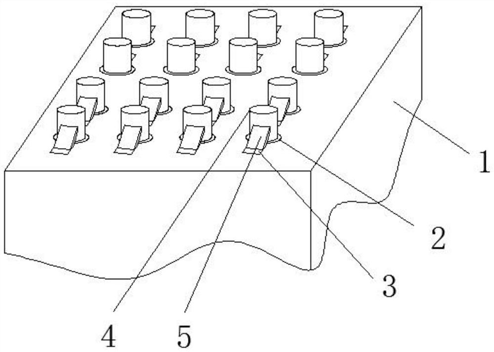
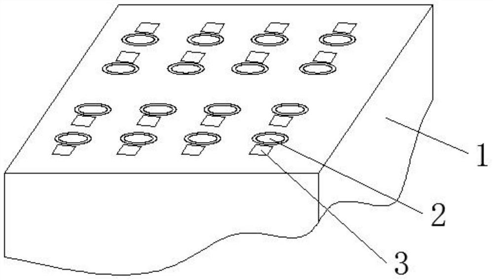
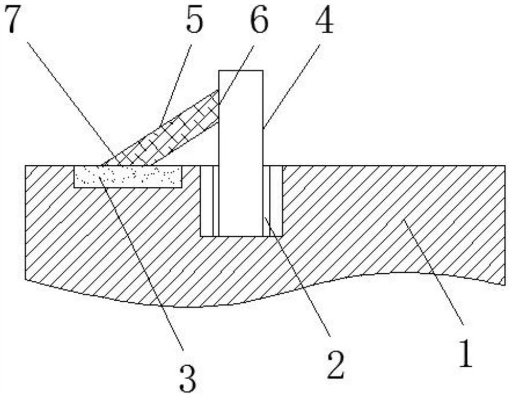
[0019] see Figure 1 to Figure 3 , the present invention provides the technical scheme of the tin connection structure of the crystal oscillator test station: the tin connection structure of the crystal oscillator test station includes a test card 1, the upper end surface of the test card 1 is provided with a test seat installation hole 2, and the test seat installation hole 2 is plugged with a test socket pin 4, one side of the test socket pin 4 is provided with a...


PUM


Abstract

The invention discloses a tin bonding connection structure of a crystal oscillator test base, and belongs to the technical field of crystal oscillator test bases. The structure includes a test card, and test seat mounting holes is formed in the upper end surface of the test card; test seat contact pins are inserted into the test seat mounting holes; test card bonding pads are arranged on one sidesof the test seat contact pins; lap soldering tin is arranged between the test seat contact pins and the test card bonding pads; the test card bonding pads are fixedly connected to the upper end surface of the test card close to the test seat mounting holes; the test seat contact pins protrude out of the test seat mounting holes; the number of the test card bonding pads is the same as that of thetest seat mounting holes, and the test card bonding pads are in one-to-one correspondence with the test seat mounting holes, a second welding foot is arranged between one end of the lap soldering tinand the test card bonding pads, tin-free via hole structures are installed on the test seat contact pins, the test seat contact pins are adjacently connected with the test card pad structure to facilitate installation and fixing of the test seat contact pins, a connection point can be conveniently and nondestructively disassembled when the test seat contact pins are maintained and disassembled, and therefore the test seat contact pins can be rapidly replaced, the contact area is large, and heat dissipation is rapid.

Description

technical field [0001] The invention relates to the technical field of a crystal oscillator test stand, in particular to a tin connection structure of a crystal oscillator test stand. Background technique [0002] As the heart of electronic equipment, the importance of crystal oscillators in equipment is self-evident; with the development of technology, crystal oscillators are gradually chipped and miniaturized, which has higher requirements for the connection structure of test tools. The test seat is installed on the test board by directly welding the test seat pins into the test card installation hole. When the test seat needs to be repaired and replaced in this way, it is necessary to absorb the welded pads one by one, remove the solder, and then The test seat can only be removed, the operation is difficult, the pad is easily damaged, and the soldering tin is arranged in the test card installation hole, which also hinders the heat dissipation effect of the device during u...

Claims


Application Information

Patent Timeline
Patent Type & Authority Applications(China)
IPC IPC(8): G01R1/04
CPCG01R1/0416
Inventor 付承
Owner 成都恒晶科技有限公司
Why Eureka
Try Eureka