Organic light-emitting display panel and preparation method

A light-emitting display and panel technology, which is applied in the manufacturing of organic semiconductor devices, semiconductor/solid-state devices, diodes, etc., can solve problems such as uneven light emission, and achieve the effect of avoiding the increase of voltage drop.

Active Publication Date: 2020-08-28
SEEYA OPTRONICS LTD
View PDF13 Cites 3 Cited by
  • Summary
  • Abstract
  • Description
  • Claims
  • Application Information

AI Technical Summary

Problems solved by technology

[0005] The embodiment of the present invention provides an organic light-emitting display panel and its preparation method, so as to prevent the cathode from being broken at the pixel defining layer, resulting in a voltage drop at the cathode and causing uneven luminescence question

Method used


Image

  • Organic light-emitting display panel and preparation method
  • Organic light-emitting display panel and preparation method
  • Organic light-emitting display panel and preparation method

Examples


Embodiment Construction

[0026] The present invention will be further described in detail below in conjunction with the accompanying drawings and embodiments. It should be understood that the specific embodiments described here are only used to explain the present invention, but not to limit the present invention. In addition, it should be noted that, for the convenience of description, only some structures related to the present invention are shown in the drawings but not all structures.

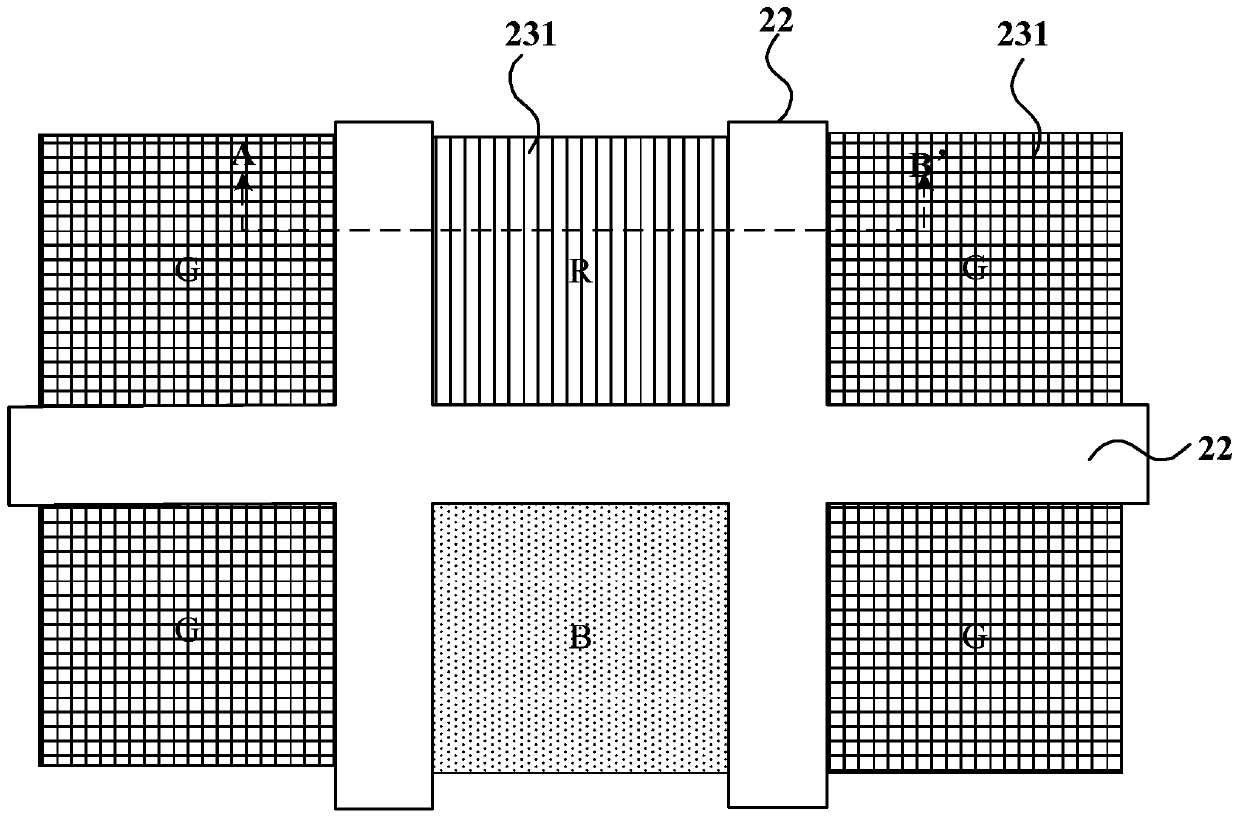
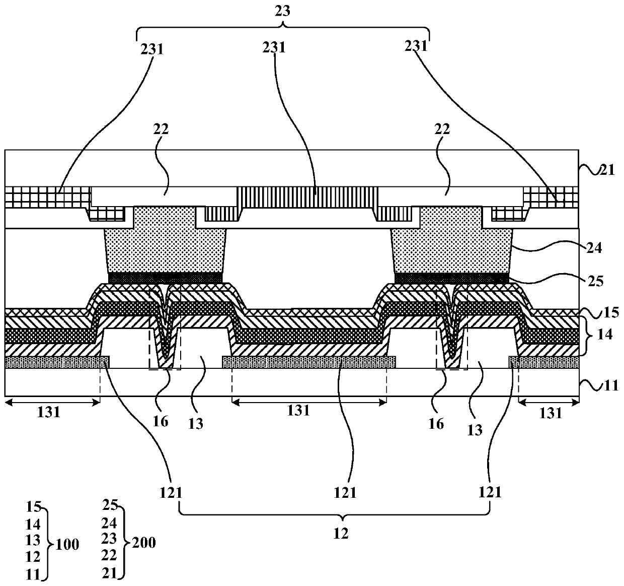
[0027] figure 1 It is a schematic structural diagram of an organic light-emitting display panel provided by an embodiment of the present invention, figure 2 yes figure 1 Provided organic light-emitting display panel along AA' sectional structure schematic diagram, such as figure 1 and figure 2 As shown, the organic light emitting display panel includes: an array substrate 100 and a color filter substrate 200 disposed opposite to each other.

[0028] The array substrate 100 includes: a first substrate 11, a f...


PUM

PropertyMeasurementUnit
diameteraaaaaaaaaa
thicknessaaaaaaaaaa
thicknessaaaaaaaaaa

Abstract

The invention discloses an organic light-emitting display panel and a preparation method. An array substrate comprises a first electrode layer, a pixel defining layer and a second electrode layer, anda first opening structure of the pixel defining layer exposes part of the first electrode; a color film substrate comprises a conductive connection structure, a color resistance layer, an elastic conductive wall and a metal connection pad; the conductive connection structure is located on the side, which faces the array substrate, of a second substrate; the color resistance layer is located on the side, which faces the array substrate, of the second substrate; a gap between adjacent sub-pixel color resistors exposes part of the conductive connection structure; the elastic conductive wall is located on the side, which faces the array substrate, of the conductive connection structure; the elastic conductive wall is in contact with the conductive connection structure through the gap betweenthe adjacent sub-pixel color resistors; the metal connection pad is located on the surface of the side, which faces the array substrate, of the elastic conductive wall; the vertical projection of theelastic conductive wall on the first substrate is overlapped with the vertical projection of the pixel defining layer on the first substrate, so that the electrical contact between the elastic conductive wall and the second electrode layer is improved, and the light emitting uniformity of the display panel is improved.

Description

technical field [0001] The invention relates to the field of display technology, in particular to an organic light-emitting display panel and a preparation method. Background technique [0002] In recent years, organic light-emitting display panels have gradually become the mainstream on mobile display terminal screens and display screens. The organic light-emitting display panel includes a plurality of sub-pixels arranged in an array, and each sub-pixel includes a pixel driving circuit and a light emitting element electrically connected to the pixel driving circuit. [0003] In the prior art, each light emitting element includes an anode, a hole auxiliary transport layer, a light emitting layer, an electron auxiliary transport layer and a cathode which are stacked. In order to increase the sub-pixel density or prepare a smaller-sized display panel, the hole-assisted transport layer, light-emitting layer, and electron-assisted transport layer of light-emitting elements of d...

Claims


Application Information

Patent Timeline
Patent Type & Authority Applications(China)
IPC IPC(8): H01L51/52H01L51/56H01L27/32
CPCH10K59/17H10K59/122H10K50/82H10K71/00H10K59/38H10K59/1315H10K50/824H10K50/856H10K59/12H10K71/60H10K71/231H10K59/1201H10K2102/3026
Inventor 黄忠守
Owner SEEYA OPTRONICS LTD
Why Eureka
Try Eureka