Efficient P-type solar cell and photovoltaic module
A solar cell, high-efficiency technology, applied in photovoltaic power generation, electrical components, circuits, etc., can solve the problem of incompatibility of the surface integrity of the emitter
- Summary
- Abstract
- Description
- Claims
- Application Information
AI Technical Summary
Problems solved by technology
Method used
Image
Examples
Embodiment approach
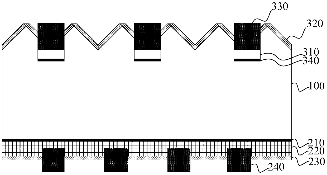
[0032] As a preferred implementation manner, the highly doped polysilicon layer 310 has a thickness ranging from 50 nanometers to 150 nanometers inclusive, such as any one of 50.0 nanometers, 100.2 nanometers or 150.0 nanometers.
[0033] In addition, the front passivation layer 320 and the back passivation layer 230 are silicon nitride layers, and the silicon nitride layer can simultaneously play anti-reflection and passivation functions, so that incident light can be better absorbed by solar cells. , improve power generation efficiency; furthermore, the thickness range of the front passivation layer 320 is 75 nanometers to 85 nanometers, such as any one of 75.0 nanometers, 80.0 nanometers or 85.0 nanometers, and the thickness range of the back passivation layer 230 is 70 nm to 90 nm, such as any of 70.0 nm, 80.0 nm or 90.0 nm, inclusive.
[0034] Also, the thickness of the N-type doped layer 220 is 50 nanometers to 150 nanometers inclusive, such as any one of 50.0 nanometers...
PUM
| Property | Measurement | Unit |
|---|---|---|
| Thickness range | aaaaa | aaaaa |
| Thickness | aaaaa | aaaaa |
| Thickness range | aaaaa | aaaaa |
Abstract
Description
Claims
Application Information
 - R&D
- Intellectual Property
- Life Sciences
- Materials
- Tech Scout
- Unparalleled Data Quality
- Higher Quality Content
- 60% Fewer Hallucinations
Browse by: Latest US Patents, China's latest patents, Technical Efficacy Thesaurus, Application Domain, Technology Topic, Popular Technical Reports.
© 2025 PatSnap. All rights reserved.Legal|Privacy policy|Modern Slavery Act Transparency Statement|Sitemap|About US| Contact US: help@patsnap.com


