
Optical fingerprint sensing device and mobile terminal

A sensing device and optical sensing technology, which is applied in the direction of acquiring/organizing fingerprints/palmprints, instruments, characters and pattern recognition, etc., can solve the problems of poor recognition accuracy of COMS optical fingerprint sensors, etc., to improve user experience, The effect of high fingerprint recognition accuracy

Pending Publication Date: 2020-08-21
GREE ELECTRIC APPLIANCES INC
View PDF6 Cites 2 Cited by
  • Summary
  • Abstract
  • Description
  • Claims
  • Application Information

AI Technical Summary

Problems solved by technology

[0005] In order to solve the technical problem of poor recognition accuracy of the COMS optical fingerprint sensor, the main purpose of this application is to provide an optical fingerprint sensor device and a mobile terminal

Method used


Image

  • Optical fingerprint sensing device and mobile terminal
  • Optical fingerprint sensing device and mobile terminal
  • Optical fingerprint sensing device and mobile terminal

Examples


Embodiment 1

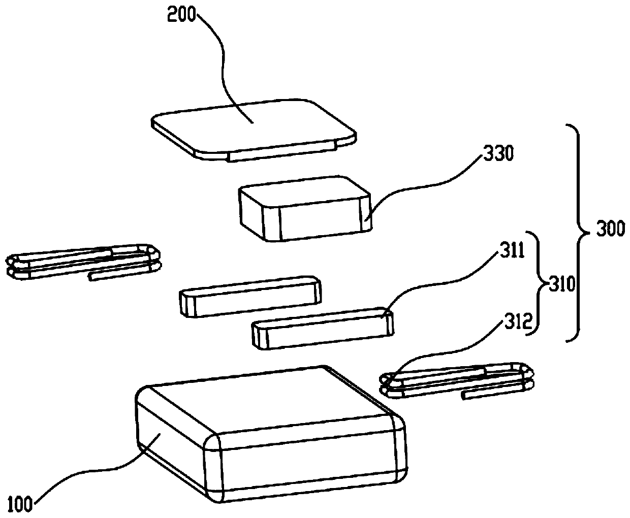
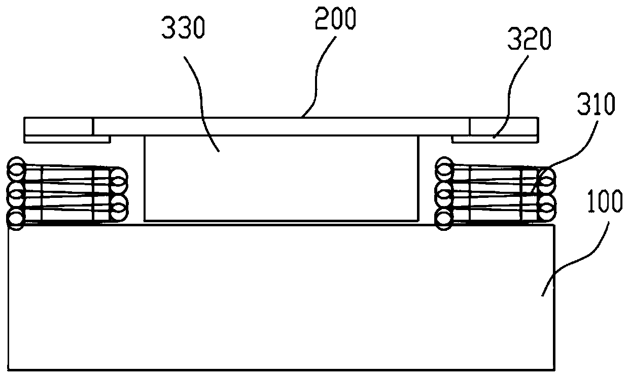
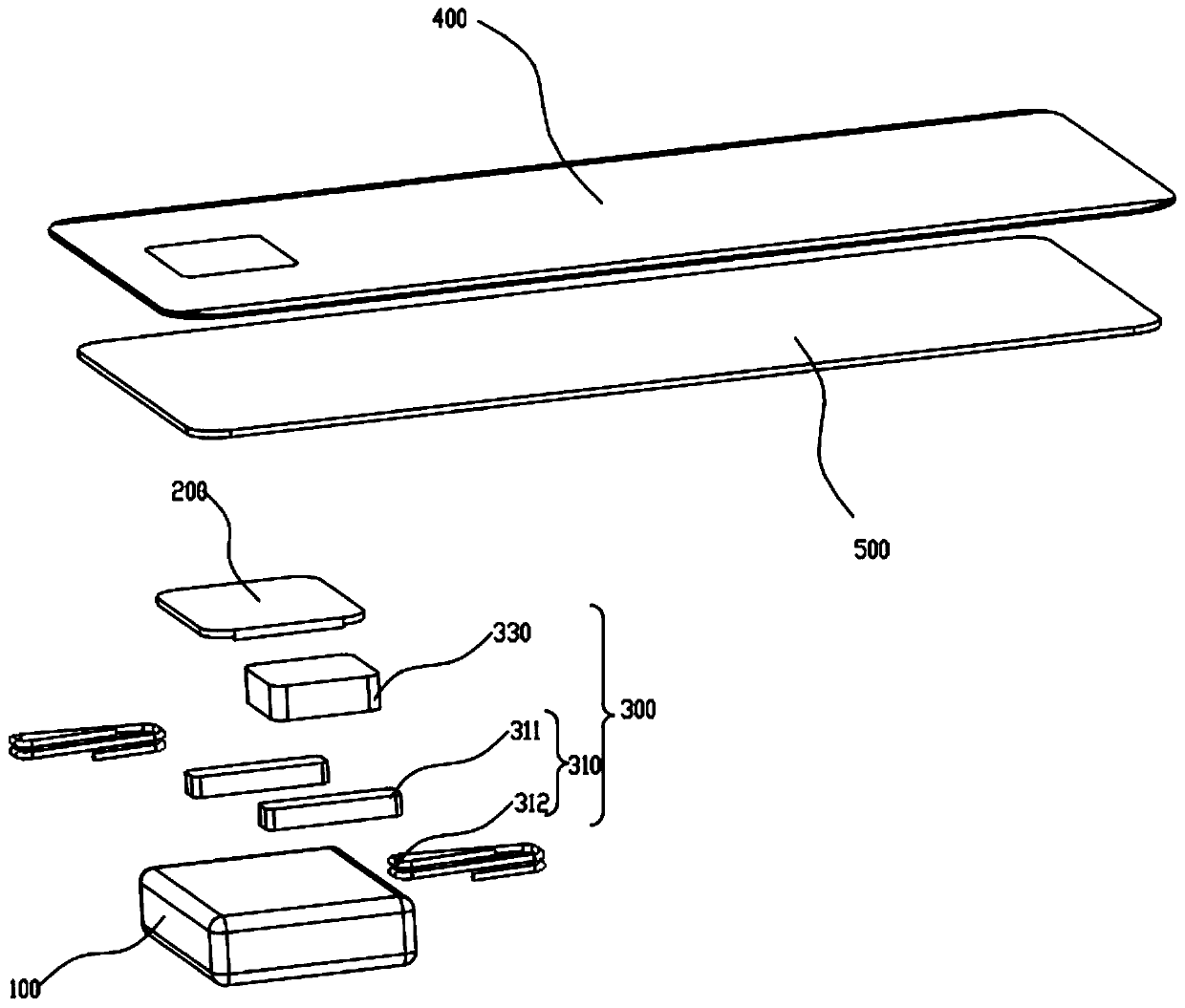
[0035] see Figure 1-2 The optical fingerprint sensing device includes an optical sensor chip 100, a photoelectric conversion element 200, and an adjustment assembly 300. The adjustment assembly 300 includes an electromagnet 310, a magnetic body 320, and a limit connector 330. The electromagnet 310 includes an iron core 311 and a coil 312. , the core 311 is mounted on the optical sensor chip 100 , and the coil 312 is wound around the core 311 .

[0036] The limit connector 330 is arranged between the optical sensor chip 100 and the photoelectric conversion part 200, and the limit connector 330 is respectively connected with the photoelectric conversion part 200 and the optical sensor chip 100, such as figure 2 As shown, the limit connector 330 has a rectangular parallelepiped structure, and the length and width of the limit connector 330 are smaller than the length and width of the optical sensor chip 100 and the photoelectric conversion element 200, leaving an installation p...


PUM


Abstract

Relating to the technical field of fingerprint identification, the invention discloses an optical fingerprint sensing device and a mobile terminal. The optical fingerprint sensing device is arranged below a screen and is used for improving fingerprint identification precision and improving experience for use. The optical fingerprint sensing device comprises an optical sensing chip and a photoelectric conversion piece. An adjusting assembly is arranged between the photoelectric conversion piece and the optical sensing chip. The optical fingerprint sensing device is arranged below the screen; the optical sensing adjusting assembly adjusts the photoelectric conversion piece to move towards and away from the screen so as to change the distance between the photoelectric conversion piece and thescreen and enable the photoelectric conversion piece to receive clear light. In order to solve the problem of the moire pattern, the adjusting assembly can control the photoelectric conversion pieceto incline relative to the screen, change the included angle between the photoelectric conversion piece and the screen, solve the problem of the moire pattern and improve the recognition precision.

Description

technical field [0001] The present application generally relates to the technical field of fingerprint identification, and in particular, relates to an optical fingerprint sensing device and a mobile terminal. Background technique [0002] At present, under-screen fingerprints have been applied to new mobile phones of major mobile phone manufacturers, mainly on OLED screens. There are mainly two types of under-screen fingerprint technology: 1. Optical sensor, which uses the principle of light reflection and refraction to feed back the texture information on the finger to the sensor in the form of light and dark stripes; 2. Ultrasonic sensor, which transmits to the finger, Ultrasound is taken to build an image. [0003] Optical sensors have a wide range of applications, but at present, in the case of interference (such as sweat stains on the screen), the recognition ability of optical sensors is limited by their own CMOS (metal oxide semiconductor, which has a photoelectric ...

Claims


Application Information

Patent Timeline
IPC IPC(8): G06K9/00
CPCG06V40/1318
Inventor 叶启璐
Owner GREE ELECTRIC APPLIANCES INC
Learn More