A 10g anti-reflection laser and its preparation process

A preparation process and anti-reflection technology, which can be applied to the structure of optical resonator cavity and the structure of optical waveguide semiconductor, and can solve problems such as disturbance.

Active Publication Date: 2021-06-08
SHANXI YUANJIE SEMICONDUCTOR TECH CO LTD +2
View PDF0 Cites 0 Cited by
  • Summary
  • Abstract
  • Description
  • Claims
  • Application Information

AI Technical Summary

Problems solved by technology

[0004] In order to solve the problem of disturbance of the active area caused by reflected light, the present invention provides a 10G anti-reflection distributed feedback laser and its preparation process, through a specific etching method and selective area growth technology (SelectiveArea Growth, SAG ), to reduce the disturbance caused by the reflected light at the light output end to the active area

Method used


Image

  • A 10g anti-reflection laser and its preparation process
  • A 10g anti-reflection laser and its preparation process
  • A 10g anti-reflection laser and its preparation process

Examples


Embodiment 1

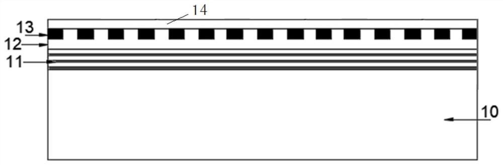
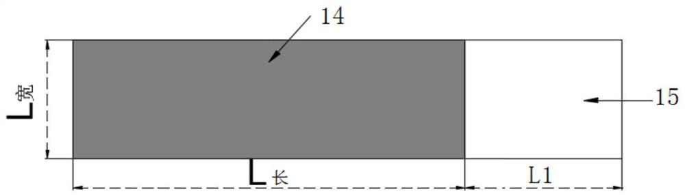
[0048] Embodiment 1: mask layer pattern size L 宽 2um, L 长 100um, lateral etching distance L 3 It is 0um, and the secondary crystal growth temperature is 650°C. L 1 20μm; L 2 is 20nm; in step 2, the etching solution ratio is Br 2 :H 3 PO 4 :H 2 O=2:1:10, the etching solution temperature is 21 degrees Celsius.

Embodiment 2

[0049] Embodiment 2: mask layer pattern size L 宽 25um, L 长 200um, lateral etching distance L 3 It is 1um, and the secondary crystal growth temperature is 700°C. L1 45μm; L 2 is 60nm; in step 2, the etching solution ratio is Br 2 :H 3 PO 4 :H 2 O=2:1:15, the temperature of the etching solution is 21.5 degrees Celsius.

Embodiment 3

[0050] Embodiment 3: mask layer pattern size L 宽 50um, L 长 300um, lateral etching distance L 3 It is 2um, and the secondary crystal growth temperature is 750°C. L 1 70μm; L 2 is 100nm; in step 2, the etching solution ratio is Br 2 :H 3 PO 4 :H 2 O=2:1:20, the temperature of the etching solution is 22 degrees Celsius.

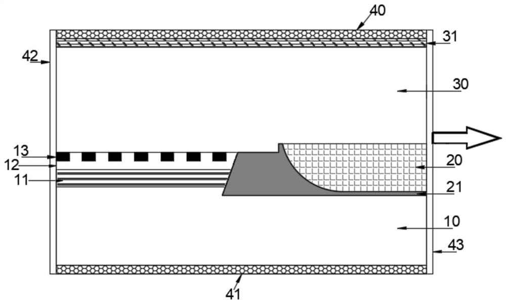
[0051] The invention discloses a preparation process of a 10G anti-reflection laser, which comprises a substrate and an active region sequentially arranged on the substrate, a first cladding layer and a diffraction grating layer, and one end of the first cladding layer and the diffraction grating layer is provided with an end face The bottom of the end-face etching area is located in the substrate, and an anti-reflection improving layer is grown in the end-face etching area; the diffraction grating layer and the anti-reflection layer are sequentially covered with a second cladding layer, a contact layer and a p-metal electrode layer, The lower surface o...


PUM

PropertyMeasurementUnit
lengthaaaaaaaaaa
distanceaaaaaaaaaa
lengthaaaaaaaaaa

Abstract

The invention discloses a 10G anti-reflection laser and a preparation process thereof. The 10G anti-reflection laser includes a substrate and an active region, a first cladding layer and a diffraction grating layer sequentially arranged on the substrate, and the first cladding layer and the diffraction grating layer One end is provided with an end face etching area, the bottom of the end face etching area is located in the substrate, and an anti-reflection improving layer is grown in the end face etching area; the diffraction grating layer and the anti-reflection layer are sequentially covered with a second cladding layer, a contact layer and a p ‑metal electrode layer, the lower surface of the substrate is coated with n‑metal electrode layer, one end of the antireflection layer is coated with an antireflection coating layer, and the other end is coated with a high reflection coating layer. The thickness of the optical waveguide layer in the docking area is thickened and the coating of the optical waveguide layer on the end face of the active area effectively improves the coupling efficiency of the active area to the optical waveguide layer; In the reverse transmission path of the laser, it can effectively attenuate to not affect the resonance behavior of the original laser gain region.

Description

technical field [0001] The invention belongs to the technical field of lasers and their preparation, and in particular relates to a 10G anti-reflection laser and a preparation process thereof. Background technique [0002] At present, the fiber-to-the-home project has been in full swing, and the commonly used edge-emitting laser is the most important optical device for the fiber-to-the-home network environment with high-speed requirements (>10Gbps). However, for edge-emitting lasers, after the laser emits light, a certain amount of light is reflected from the system link back to the chip end, which will inevitably affect the performance of the high-speed laser. In order to avoid this problem, in the process of chip packaging, It is necessary to add an optical isolator to block the reflected light, but the optical isolator mainly depends on imports and is expensive, so adding an optical isolator increases the construction cost. For this kind of problem, the patent "a 10G ...

Claims


Application Information

Patent Timeline
Patent Type & Authority Patents(China)
IPC IPC(8): H01S5/12H01S5/22
CPCH01S5/12H01S5/22
Inventor 董延李马惠潘彦廷
Owner SHANXI YUANJIE SEMICONDUCTOR TECH CO LTD
Why Eureka
Try Eureka