Integrated bypass protection device for field of solar energy and process method thereof
A technology for bypass protection and device protection, which is applied in the manufacture of semiconductor devices, electrical solid state devices, and semiconductor/solid state devices. Product heat dissipation area, enhanced product reliability, and stable product performance
- Summary
- Abstract
- Description
- Claims
- Application Information
AI Technical Summary
Problems solved by technology
Method used
Image
Examples
Embodiment 1
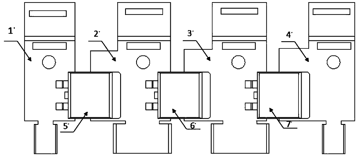
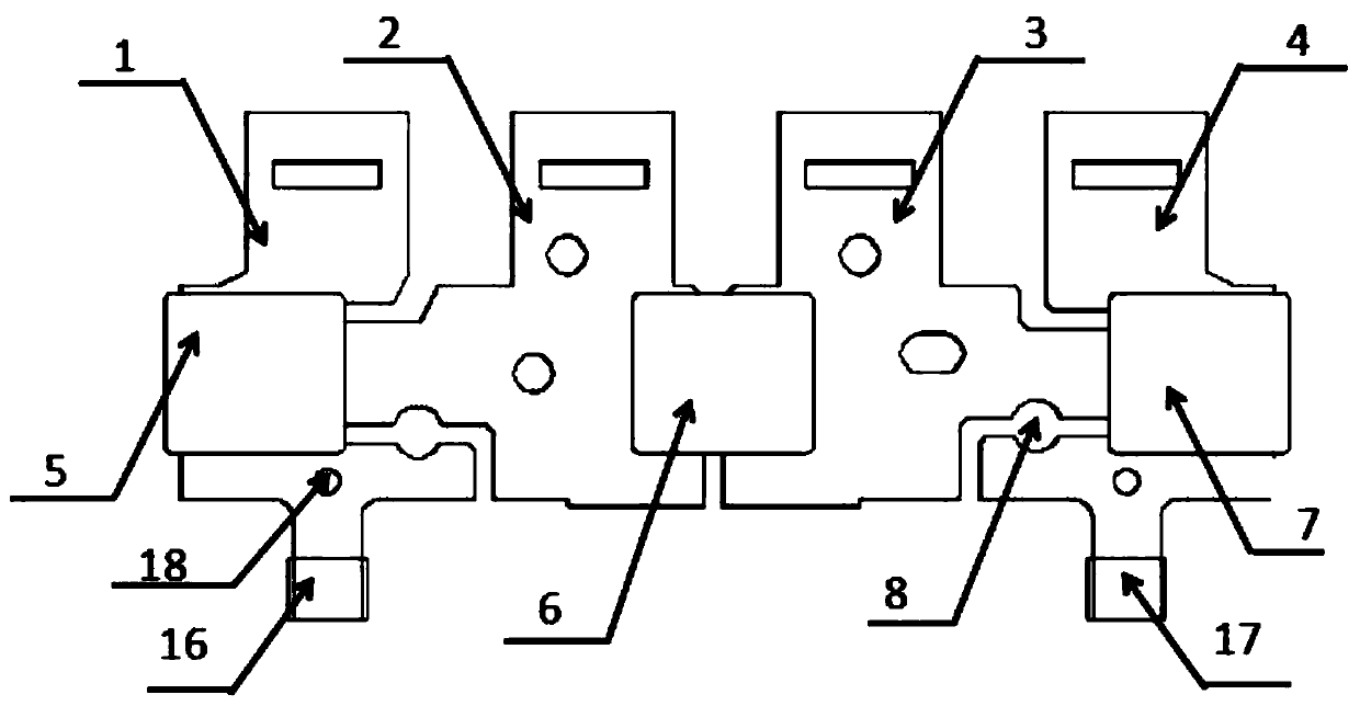
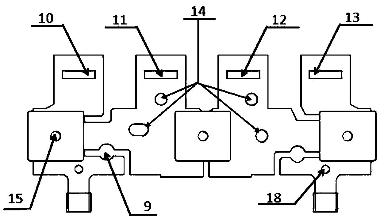
[0048] Such as Figure 1-8 As shown, the integrated bypass protection device used in the field of solar energy according to the present invention includes a frame. Form an integral structure with the frame on the frame, a photovoltaic chip 23 is arranged in the plastic package of the protection device, a chip pad 21 and a jumper pad 20 are arranged above the frame, and the photovoltaic chip 23, the chip pad 21 and the jumper pad 20 are arranged Inside the protective device plastic package, the photovoltaic chip 23 is connected to the chip pad 21, the photovoltaic chip 23 is connected to the jumper pad 20 through the jumper 19, the outside of the frame is connected to the anode pin 16 and the cathode pin 17, and the anode lead The pin 16 and the cathode pin 17 are respectively connected to the photovoltaic cell, and the frame carries and communicates with the photovoltaic chip 23 and the internal and external circuits to form an integrated bypass protection device.
[0049]The...
Embodiment 2
[0070] Embodiment 2: The process method of the integrated bypass protection device used in the field of solar energy according to the present invention comprises the following steps:
[0071] Step 1: Raw material preparation:
[0072] Prepare frame, photovoltaic chip, epoxy molding compound, solder paste, jumper wire;
[0073] Step 2: Mounting and welding:
[0074] Weld the loaded frame, photovoltaic chip and jumper together by welding furnace welding;
[0075] Step 3: Shaping:
[0076] The semi-finished products after assembly and welding are plastic-sealed and molded by plastic sealing;
[0077] Step 4: Post Curing:
[0078] Baking in an oven is used to fully cure the formed semi-finished product and eliminate packaging stress;
[0079] Step 5: Trim the tendons and bend the corners:
[0080] Use mechanical punching to remove the excess frame, and stamp the pins into a fixed shape;
[0081] Step 6: Test Printing:
[0082] Use TMTT testing machine to point out electric...
PUM
 Abstract
Description
Claims
Application Information
 - R&D
- Intellectual Property
- Life Sciences
- Materials
- Tech Scout
- Unparalleled Data Quality
- Higher Quality Content
- 60% Fewer Hallucinations
Browse by: Latest US Patents, China's latest patents, Technical Efficacy Thesaurus, Application Domain, Technology Topic, Popular Technical Reports.
© 2025 PatSnap. All rights reserved.Legal|Privacy policy|Modern Slavery Act Transparency Statement|Sitemap|About US| Contact US: help@patsnap.com


