Manufacturing method of low-voltage high-density trench DMOS device

A device manufacturing method and high-density technology, applied in semiconductor/solid-state device manufacturing, semiconductor devices, electrical components, etc., can solve the problems of being easily pierced by holes and low product yield, and reduce the short circuit problem of polysilicon through the gate , Improve product yield and reliability, optimize process effect

Active Publication Date: 2020-08-07
58TH RES INST OF CETC
View PDF5 Cites 0 Cited by
  • Summary
  • Abstract
  • Description
  • Claims
  • Application Information

AI Technical Summary

Problems solved by technology

[0003] The purpose of the present invention is to provide a low-voltage high-density trench DMOS device manufacturing method to solve the problem that the current process is easily pierced by the hole when the gate polysilicon leads to the contact hole, resulting in low product yield.

Method used


Image

  • Manufacturing method of low-voltage high-density trench DMOS device
  • Manufacturing method of low-voltage high-density trench DMOS device
  • Manufacturing method of low-voltage high-density trench DMOS device

Examples


Embodiment 1

[0031] The invention provides a method for manufacturing a low-voltage high-density trench DMOS device, comprising the steps of:

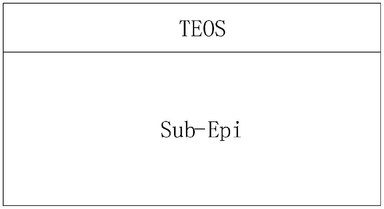
[0032] Deposit a layer of oxide layer on a suitable epitaxial material. In the first embodiment, silicon is selected as the epitaxial material, and the deposited oxide layer is TEOS material. The height of the TEOS material is 4000~8000Å, such as figure 1 shown;

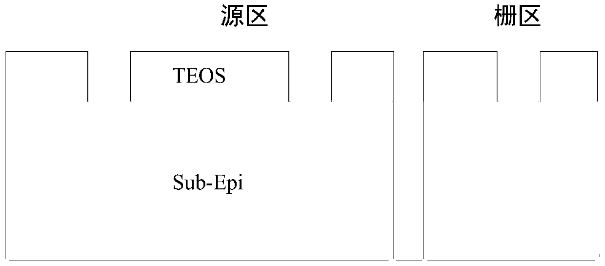
[0033] Using photolithography and dry etching process on the silicon material, first etch the oxide layer, such as figure 2 shown;

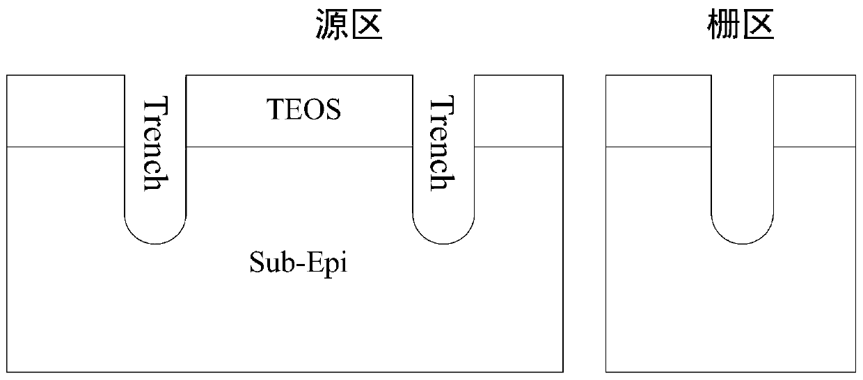
[0034] Use the remaining oxide layer as a mask layer to etch the trench array, such as image 3 ;

[0035] Retain the oxide layer as a masking layer, remove the surface silicon damage in the trench array through a sacrificial oxidation process, use thermal oxidation to grow a gate oxide layer with a certain thickness, and deposit polysilicon gate Poly in the trench array, such as Figure 4 shown;

[0036] Use the dry etching back process to etch away t...


PUM

PropertyMeasurementUnit
heightaaaaaaaaaa

Abstract

The invention discloses a manufacturing method of a low-voltage high-density trench DMOS device, which belongs to the technical field of semiconductor power devices. After the trench array is completed, sacrificial oxidation to repair the damage of the inner surface of the trench array is directly performed without removing the oxide layer. The surface of the polycrystalline silicon in the trencharray is 2000-3000 angstroms higher than the surface of the silicon. And through an oxide layer etching technology, the oxide layer on the surface of the silicon is removed through dry etching, and the residual oxide layer with a certain thickness is taken as a well injection barrier layer. The masking oxide layer in trench array etching is used for raising the height of the polysilicon at the gate lead-out position, so that the polysilicon is prevented from being perforated by hole corrosion, and the product yield and reliability are improved; by optimizing the process, the problem of short circuit of gate polycrystalline silicon perforated through a gate contact hole is reduced, so that the product yield and the reliability are improved.

Description

technical field [0001] The invention relates to the technical field of semiconductor power devices, in particular to a method for manufacturing a low-voltage high-density trench DMOS device. Background technique [0002] With the continuous expansion of the application field of VDMOS products and the continuous improvement of process line capabilities, the industry's requirements for product energy efficiency are also getting higher and higher. Ordinary low-voltage Trench DMOS products, because the channel resistance accounts for a large proportion, the optimization direction is to reduce the size of the original cell and the shallow junction process of the channel. Taking N20V products as an example, the original cell unit of mass products on the market has been reduced to 0.9um, and the well depth is about 0.5~0.7um. The gate electrode of this product is generally drawn out at the edge of the die through a large trench. Under the current process conditions, due to the hig...

Claims


Application Information

Patent Timeline
Patent Type & Authority Applications(China)
IPC IPC(8): H01L21/28H01L21/336
CPCH01L29/66734H01L29/401
Inventor 廖远宝洪根深吴建伟吴锦波徐政徐海铭
Owner 58TH RES INST OF CETC
Why Eureka
Try Eureka