
Processing method for preventing pad from falling off in packaging process of multilayer thick circuit board

A processing method and circuit board technology, which can be used in multilayer circuit manufacturing, printed circuit manufacturing, printed circuit manufacturing, etc., and can solve the problems of reduced array density, wasted cost, and increased pad size.

Active Publication Date: 2020-07-28
WUS PRINTED CIRCUIT (KUNSHAN) CO LTD
View PDF4 Cites 0 Cited by
  • Summary
  • Abstract
  • Description
  • Claims
  • Application Information

AI Technical Summary

Problems solved by technology

Existing method wastes cost, increasing pad size leads to reduced array density

Method used


Image

  • Processing method for preventing pad from falling off in packaging process of multilayer thick circuit board

Examples


Embodiment Construction

[0017] The present invention will be further described below in conjunction with the accompanying drawings.

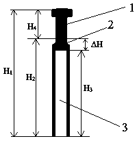
[0018] A processing method for solving the problem of pad drop in the packaging process of a multilayer thick circuit board. The multilayer thick circuit board is provided with an all-copper via hole 1, and a back-drilled hole 2 arranged at the all-copper via hole 1, including The process is as follows: fill the back-drilled hole 2 with resin, and back-drill air holes 3 at the resin after the resin is cured.

[0019] The diameter of the air hole 3 is smaller than that of the back-drilled hole 2 .

[0020] There is a height difference between the air hole 3 and the back-drilled hole 2, and the height difference is the thermal expansion compensation height ΔH.

[0021] The thermal expansion compensation height ΔH = back drilling height H 2 -Stomatal height H 3 ;

[0022] The stomatal height H 3 ={[(Expansion volume of residual copper in via + CTE expansion volume be...


PUM


Abstract

The invention discloses a processing method for preventing a pad from falling off in the packaging process of a multilayer thick circuit board. The multilayer thick circuit board is provided with an all-copper via hole and a back drill hole arranged at the all-copper via hole. The processing method comprises the following steps: filling the back drill hole with resin, and after the resin is cured,drilling an air vent at the back drill hole in a back drilling manner. According to the method, the air vent is drilled in the resin to compensate the difference value of the expansion volumes of theall-copper via hole and the resin of the back drill hole, so the expansion volumes of the back drill hole and the all-copper via hole are consistent, and the problem that the pad falls off in the process of cooling after the circuit board is welded and packaged is solved.

Description

technical field [0001] The invention relates to a processing method for solving the problem of missing pads during the packaging process of multilayer thick circuit boards, and belongs to the technical field of printed circuit boards. Background technique [0002] In consideration of signal transmission, the communication design needs to reduce the insertion loss of the hole. The back-drilling area of ​​the BGA area is mostly designed to reduce the crosstalk of the hole wall to the signal. There is a difference in CTE expansion in the hole area during the soldering process, and the expansion volume of the all-copper hole is smaller than that of the back-drilled hole area, so that the PAD phenomenon will appear during the cooling process of the circuit board after soldering. At present, the methods to solve this problem mainly include: changing the design scheme, increasing the size of the pad; reworking and planting balls for the defective chips caused by welding. The exist...

Claims


Application Information

Patent Timeline
Patent Type & Authority Applications(China)
IPC IPC(8): H05K3/46H05K3/42
CPCH05K3/4611H05K3/4614H05K3/429H05K3/421
Inventor 琼迪克森吴传彬
Owner WUS PRINTED CIRCUIT (KUNSHAN) CO LTD
Learn More