Array substrate and manufacturing method thereof

A technology of an array substrate and a manufacturing method, applied in the display field, can solve the problems of slow etching speed, excessive CDloss of copper conductive layer, low aperture ratio, etc., achieves small loss of line width, shortens wet etching time, and improves opening rate effect

Inactive Publication Date: 2020-07-24
SHENZHEN CHINA STAR OPTOELECTRONICS TECH CO LTD
View PDF6 Cites 1 Cited by
  • Summary
  • Abstract
  • Description
  • Claims
  • Application Information

AI Technical Summary

Problems solved by technology

[0006] The array substrate and the manufacturing method thereof provided by the present invention solve the problem that the etching speed of the liner layer is relatively slow under the existing etching solution system in the existing manufacturing method of the array substrate, which causes the CD loss of the copper conductive layer to be too large, and further Technical problems leading to low aperture ratio

Method used


Image

  • Array substrate and manufacturing method thereof
  • Array substrate and manufacturing method thereof
  • Array substrate and manufacturing method thereof

Examples


Embodiment Construction

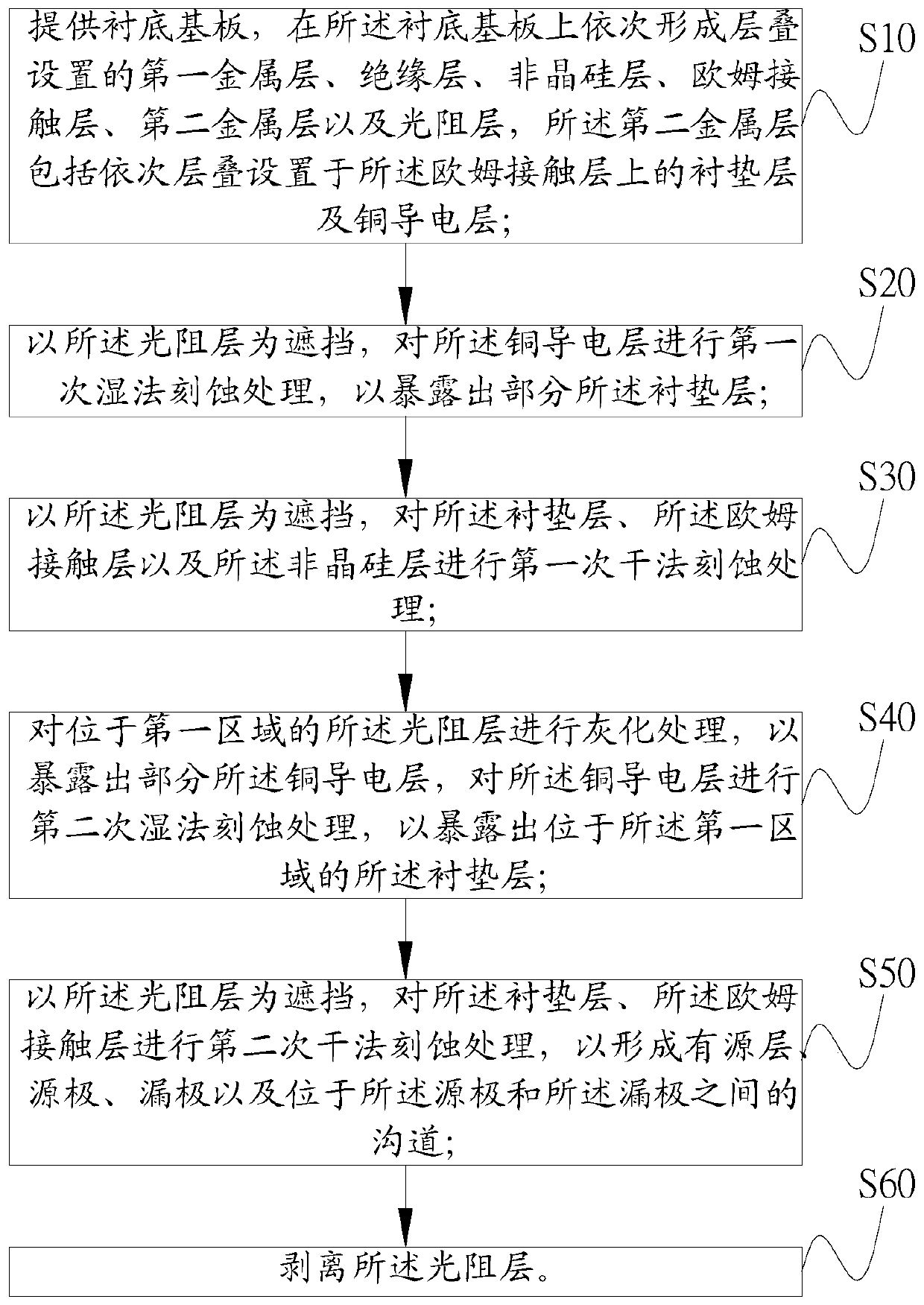
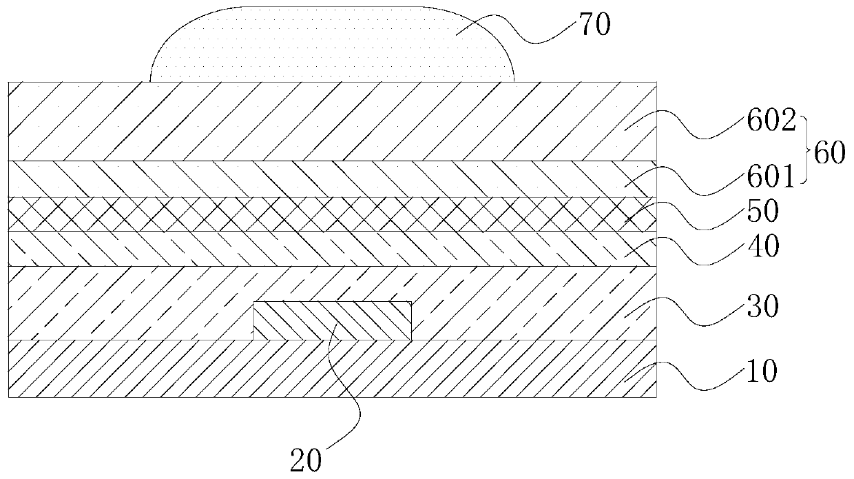
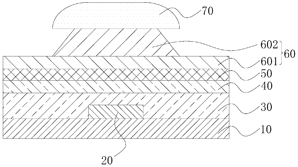
[0036] The following descriptions of the various embodiments refer to the accompanying drawings to illustrate specific embodiments in which the invention may be practiced. The directional terms mentioned in the present invention, such as [top], [bottom], [front], [back], [left], [right], [inside], [outside], [side], etc., are only for reference The orientation of the attached schema. Therefore, the directional terms used are used to illustrate and understand the present invention, but not to limit the present invention. In the figures, structurally similar elements are denoted by the same reference numerals.

[0037] In the description of the present application, it should be understood that the terms "center", "longitudinal", "transverse", "length", "width", "thickness", "upper", "lower", "front", " Orientation indicated by rear, left, right, vertical, horizontal, top, bottom, inside, outside, clockwise, counterclockwise, etc. The positional relationship is based on the or...


PUM


Abstract

The invention provides an array substrate and a manufacturing method thereof. In the manufacturing method of the array substrate, when a second metal layer is subjected to first wet etching treatmentand second wet etching treatment, wet etching treatment is stopped only after etching of a copper conductive layer is completed, molybdenum of a liner layer is completely reserved at the moment, and due to a fact that a wet etching speed of the liner layer is low, wet etching time can be greatly shortened, CD loss of the copper conductive layer is greatly reduced, and line width losses are small;and meanwhile, a step of etching the liner layer is added in a traditional dry etching process so that the overall CD loss of the second metal layer can be reduced, the metal line width loss is decreased, and an aperture opening ratio is improved.

Description

technical field [0001] The present invention relates to the field of display technology, in particular to an array substrate and a manufacturing method thereof. Background technique [0002] Thin film transistor liquid crystal display (TFT-LCD) occupies a dominant position in the current flat panel display market due to its small size, low power consumption, and no radiation. At present, the 4mask (mask) process is widely used in the industry and has obvious savings. Process effect. [0003] With the continuous upgrading of panel requirements, 8K has become the main direction for the development of large-size panels. The improvement of resolution and size makes copper process not only a must-use technology, but also copper thickness is getting bigger and bigger. The copper process structure is generally composed of a copper conductive layer and a liner layer (usually molybdenum or titanium). Since the etching speed of the liner layer is relatively slow under the existing et...

Claims


Application Information

Patent Timeline
Patent Type & Authority Applications(China)
IPC IPC(8): H01L27/12H01L21/77G02F1/1362
CPCH01L27/1214H01L27/1259G02F1/1362H01L21/32134H01L21/32135H01L21/32139H01L29/66765H01L27/1288H01L29/78618H01L21/30604H01L21/3081H01L27/1225H01L29/7869
Inventor 谭志威
Owner SHENZHEN CHINA STAR OPTOELECTRONICS TECH CO LTD
Why Eureka
Try Eureka