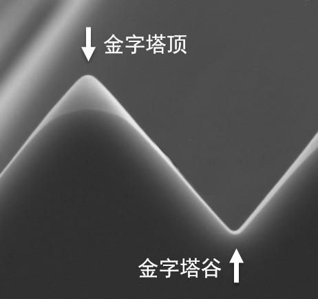
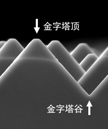
Silicon wafer texturing method
A silicon wafer and silicon wafer surface technology, applied in the field of battery preparation technology, can solve the problems of the influence of amorphous silicon deposition, the ability to peel off particles is not fully reflected, and the organic residues, etc. The effect of reflectivity
- Summary
- Abstract
- Description
- Claims
- Application Information
AI Technical Summary
Problems solved by technology
Method used
Image
Examples
Embodiment 1
[0033] A kind of texturing method of silicon chip, comprises the following steps:
[0034] S1. Carry out pre-oxidation treatment to the silicon wafer to be treated to remove the surface pollutants of the silicon wafer. The used cleaning solution SC1 solution, wherein the volume fraction of the KOH solution with a concentration of 45wt% is 1.6%, and the concentration is 30wt% of H 2 o 2 The volume fraction of the aqueous solution is 10%, the balance is water, the temperature is 60°C, and the time is 5 minutes;
[0035] S2. Put the silicon wafer obtained in S1 into pure water for cleaning, and wash off the cleaning solution in S1 remaining on the surface of the silicon wafer;
[0036] S3. Put the silicon wafer obtained in S2 into the SDE tank for damage removal treatment. The solution in the SDE tank has a concentration of 20 wt% KOH solution, the balance is water, the temperature is 70°C, and the treatment time is 30s;
[0037] S4, putting the silicon wafer obtained in S3 int...
Embodiment 2
[0047] A kind of texturing method of silicon chip, comprises the following steps:
[0048] S1, carrying out pre-oxidation treatment to the silicon wafer to be treated to remove the surface pollutants of the silicon wafer, the cleaning solution SC1 solution used, wherein the volume fraction of the NaOH solution with a concentration of 45wt% is 1.6%, and the concentration is 30wt% of H 2 o 2 The volume fraction of the aqueous solution is 10%, the balance is water, the temperature is 60°C, and the time is 5 minutes;
[0049] S2. Put the silicon wafer obtained in S1 into pure water for cleaning, and wash off the cleaning solution in S1 remaining on the surface of the silicon wafer;
[0050] S3. Put the silicon wafer obtained in S2 into the SDE tank for damage removal treatment. The solution in the SDE tank has a concentration of 10 wt% KOH solution, the balance is water, the temperature is 42°C, and the treatment time is 100s;
[0051] S4, putting the silicon wafer obtained in S...
Embodiment 3
[0061] A kind of texturing method of silicon chip, comprises the following steps:
[0062] S1, pre-oxidize the silicon wafer to be treated to remove the surface pollutants of the silicon wafer, the cleaning solution SC1 solution used, wherein the concentration is 45wt% NH 4 The OH solution has a volume fraction of 1.6% and a concentration of 30 wt% H 2 o 2 The volume fraction of the aqueous solution is 10%, the balance is water, the temperature is 60°C, and the time is 5 minutes;
[0063] S2. Put the silicon wafer obtained in S1 into pure water for cleaning, and wash off the cleaning solution in S1 remaining on the surface of the silicon wafer;
[0064] S3. Put the silicon wafer obtained in S2 into the SDE tank for damage removal treatment. The solution in the SDE tank is a KOH solution with a concentration of 2wt%, the balance is water, the temperature is 85°C, and the treatment time is 240s;
[0065] S4, putting the silicon wafer obtained in S3 into O 3 Washed in solutio...
PUM
 Abstract
Description
Claims
Application Information
 - R&D Engineer
- R&D Manager
- IP Professional
- Industry Leading Data Capabilities
- Powerful AI technology
- Patent DNA Extraction
Browse by: Latest US Patents, China's latest patents, Technical Efficacy Thesaurus, Application Domain, Technology Topic, Popular Technical Reports.
© 2024 PatSnap. All rights reserved.Legal|Privacy policy|Modern Slavery Act Transparency Statement|Sitemap|About US| Contact US: help@patsnap.com


