Storage structure and preparation method thereof

A storage structure and stacking structure technology, applied in the direction of semiconductor devices, electrical components, circuits, etc., can solve the problems of increased step area, UCH-LCH and C1CH-UCH alignment difficulties, etc., to reduce the occupied area and process Difficulty and cost, and the effect of reducing the occupied area of ​​steps

Active Publication Date: 2021-08-13
YANGTZE MEMORY TECH CO LTD
View PDF7 Cites 0 Cited by
  • Summary
  • Abstract
  • Description
  • Claims
  • Application Information

AI Technical Summary

Problems solved by technology

[0005] In view of the above-mentioned shortcomings of the prior art, the object of the present invention is to provide a storage structure and its preparation method, which are used to solve the UCH-LCH and C1CH-UCH alignment difficulties existing in the storage structure in the prior art, and Problems with increasing step size

Method used


Image

  • Storage structure and preparation method thereof
  • Storage structure and preparation method thereof
  • Storage structure and preparation method thereof

Examples


Embodiment Construction

[0095] Embodiments of the present invention are described below through specific examples, and those skilled in the art can easily understand other advantages and effects of the present invention from the content disclosed in this specification. The present invention can also be implemented or applied through other different specific implementation modes, and various modifications or changes can be made to the details in this specification based on different viewpoints and applications without departing from the spirit of the present invention.

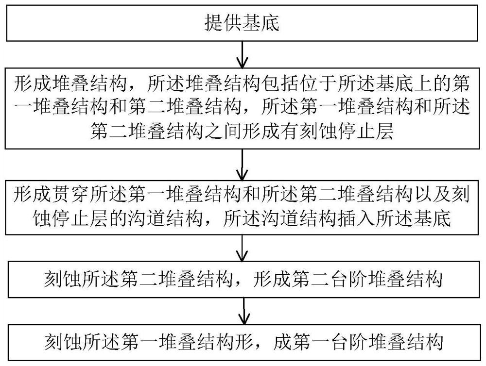
[0096] see Figure 1 to Figure 11 . It should be noted that the diagrams provided in this embodiment are only schematically illustrating the basic idea of ​​the present invention, and only the components related to the present invention are shown in the diagrams rather than the number, shape and shape of the components in actual implementation. Dimensional drawing, the type, quantity and proportion of each component can be changed ar...


PUM


Abstract

The present invention provides a storage structure and a preparation method thereof. A first stacked structure and a second stacked structure are respectively formed on opposite sides of an etching stop layer, and a channel structure is prepared first, followed by a second stepped stacked structure and a second stacked structure. A step stack structure can effectively solve the difficulties in aligning the first channel structure and the second channel structure, the difficulty in aligning the channel local contact and the second channel structure, and the common source local contact and slit caused by the step process. structure alignment is difficult; and the present invention can reduce the area occupied by the steps, and prepare a high-density, highly integrated storage structure; further, the present invention draws the common source from the substrate side by preparing a pseudo-slit structure, which can be obtained from Fundamentally solve the problem of difficult alignment between the local contact of the common source and the slit structure, reduce the difficulty and cost of the process, and reduce the occupied area of ​​the slit structure.

Description

technical field [0001] The invention belongs to the field of semiconductor design and manufacture, and relates to a storage structure and a preparation method thereof. Background technique [0002] With the development of technology, the semiconductor industry is constantly looking for new production methods so that each memory die in a memory device has a greater number of memory cells. In non-volatile memory, such as NAND memory, one way to increase memory density is through the use of vertical memory arrays, and with the increase in integration, the number of memory layers has grown from 32 layers to 64 layers, or even higher the number of layers. [0003] In the existing storage structure preparation process, it mainly includes the following processes: lower step (LSS)-lower channel (LCH)-upper step (USS)-upper channel (UCH)-slot structure (GL)-lower step Contact (LCT)-Upper Step Contact (UCT)-Partial Contact (C1CH and C1ACS)-Contact (V0). However, as the number of la...

Claims


Application Information

Patent Timeline
Patent Type & Authority Patents(China)
IPC IPC(8): H01L27/1157H01L27/11582
CPCH10B43/35H10B43/27
Inventor 徐伟杨星梅王健舻吴继君黄攀周文斌
Owner YANGTZE MEMORY TECH CO LTD
Why Eureka
Try Eureka