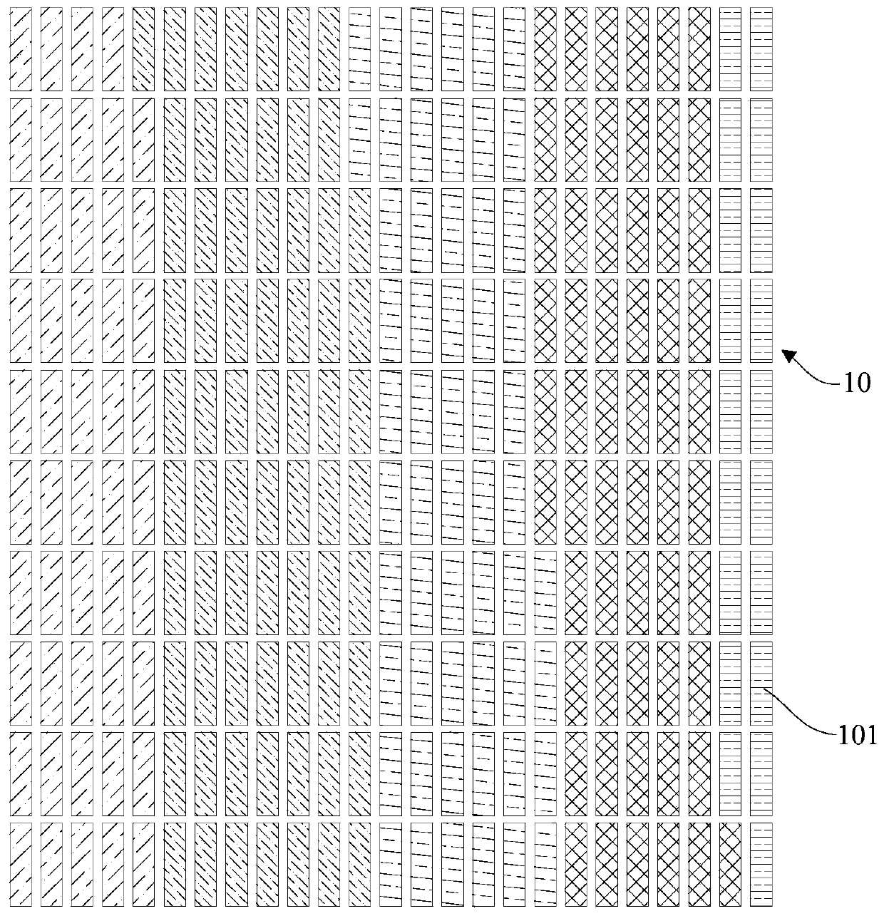
LED display screen and manufacturing method thereof
A technology of LED display screen and manufacturing method, which is applied in the fields of semiconductor/solid-state device manufacturing, transportation and packaging, semiconductor devices, etc., can solve the problems of incompleteness, low production efficiency, differences, etc. Effect
- Summary
- Abstract
- Description
- Claims
- Application Information
AI Technical Summary
Problems solved by technology
Method used
Image
Examples
Embodiment 1
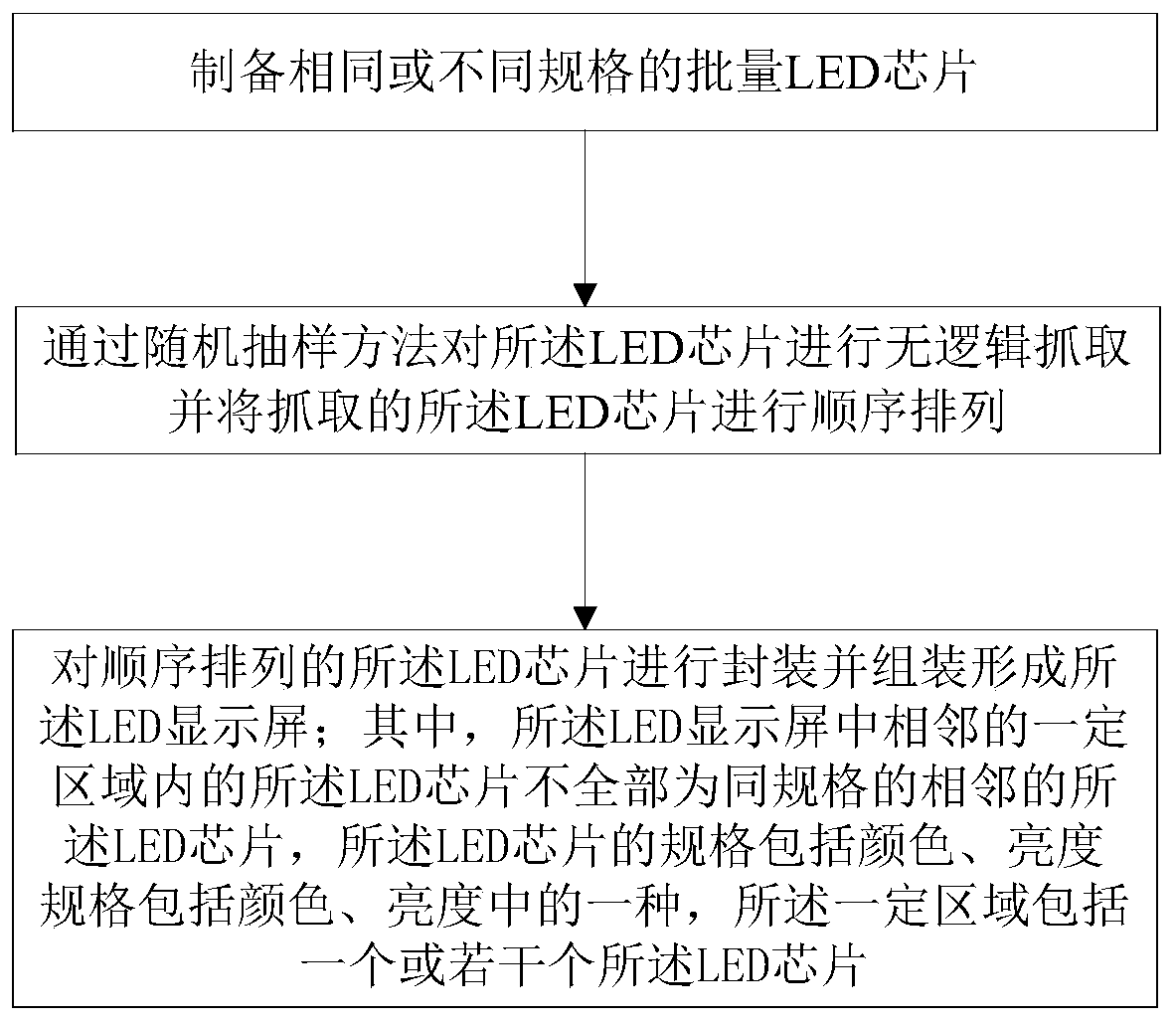
[0061] In order to solve the problem of brightness difference and color difference between the screens caused by LED sorting in the above-mentioned prior art, this embodiment provides a method for manufacturing an LED flip-chip display screen, such as Figure 2-6 shown, including the following steps:
[0062] Prepare batches of LED chips with the same or different specifications;
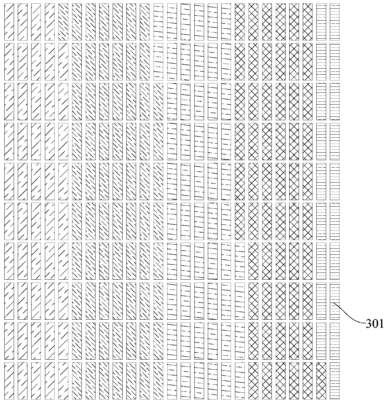
[0063] The aforementioned LED chips with the same or different specifications may come from the same wafer or different wafers. In a preferred embodiment of this embodiment, as image 3 As shown, LED chips 301 of the same specification from different wafers are divided into different bins. In an optional embodiment of this embodiment, the LED chips can also be divided into LED chips with the same bin but different brightness or wavelength. In this embodiment, the specification of the LED chip 301 includes at least one of color or brightness.
[0064] Grabbing the aforementioned batches of LED ch...
Embodiment 2
[0081] This embodiment provides a method for manufacturing an LED flip-chip display screen, and the similarities with Embodiment 1 will not be repeated, and the difference lies in:
[0082] In this embodiment, the LED chips can be grabbed illogically from the wafer on which the LED chips are cut out by random sampling method; Any sticky carrier film such as white film, PVC film, etc.; then transfer the LED chips on the carrier film to the circuit substrate in batches; package and assemble the LED chips transferred to the circuit substrate to form an LED display.
[0083] The method shown in the above-mentioned embodiments of the present invention can directly carry out illogical grabbing and then arrange LED chips of the same or different specifications from the same wafer, so the method can directly grab the LED chips without binning, and realize LED chips Scattered and evenly distributed. In addition, this method can also grab and arrange LED chips of the same specification...
Embodiment 3
[0087] This embodiment provides an LED display screen, which includes a display unit, and the display unit includes a circuit substrate and an LED chip welded on the circuit substrate;
[0088] Wherein, the LED chips include LED chips from the same wafer and / or LED chips from different wafers, the LED chips are randomly arranged and welded on the circuit substrate, and the adjacent LED chips are not It includes adjacent LED chips with the same specification, and the specification of the LED chip includes at least one of chromaticity and brightness of the LED chip.
[0089] In a preferred embodiment of this embodiment, the LED chips include flip-chip Mini LED chips or Micro LED chips.
[0090] In another preferred embodiment of this embodiment, the LED display screen further includes a control system, which is electrically connected to the display unit to control the display unit to display according to different requirements.
[0091] In the LED display screen of this embodimen...
PUM
 Abstract
Description
Claims
Application Information
 - R&D Engineer
- R&D Manager
- IP Professional
- Industry Leading Data Capabilities
- Powerful AI technology
- Patent DNA Extraction
Browse by: Latest US Patents, China's latest patents, Technical Efficacy Thesaurus, Application Domain, Technology Topic, Popular Technical Reports.
© 2024 PatSnap. All rights reserved.Legal|Privacy policy|Modern Slavery Act Transparency Statement|Sitemap|About US| Contact US: help@patsnap.com


