Graphene transistor label-free glucose sensor and preparation method thereof
A graphene and transistor technology, applied in the field of biosensors, can solve the problems of time-consuming, expensive instruments, etc., and achieve the effects of high sensitivity, low cost, and lower operating voltage
- Summary
- Abstract
- Description
- Claims
- Application Information
AI Technical Summary
Problems solved by technology
Method used
Image
Examples
preparation example Construction
[0037] The present invention also provides a preparation method for the graphene transistor sensor described in the above technical solution, comprising the following steps:
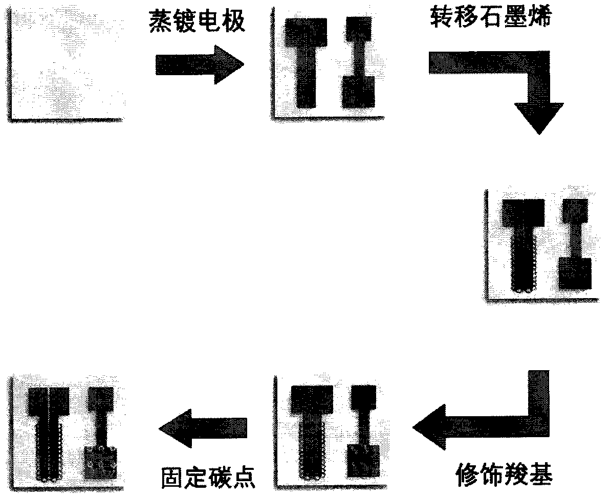
[0038] (1) Prepare gate, source and drain on the surface of the substrate, so that there is a channel between the source and drain;
[0039] (2) Graphene is tiled on the channel between the source and the drain to obtain a graphene transistor;
[0040](3) carbon dots are fixed on the grid surface of the graphene transistor obtained in the step (2), to obtain a graphene transistor sensor.
[0041] In the present invention, gate, source and drain are prepared on the substrate surface, so that a channel exists between the source and drain. In the present invention, the preparation of the gate electrode, the source electrode and the drain electrode preferably includes: sequentially vapor-depositing a chromium layer and a gold layer on the surface of the substrate by a thermal evaporation coating method.
...
Embodiment 1
[0067] Thermal evaporation coating:
[0068] Cut the electronic grade glass into 12×12mm size, ultrasonically clean it with acetone, isopropanol, and ethanol for ten minutes, dry it in an oven, paste the glass piece on a mask plate of a specific shape with high-temperature glue, and weigh an appropriate amount The chromium and gold are put into the tungsten boat to prepare the vacuum thermal evaporation coating.
[0069] When evaporating, first evaporate chromium: the thickness is 8nm.
[0070] Evaporation gold layer again: the thickness is 50nm.
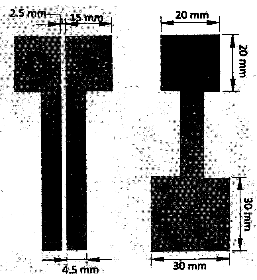
[0071] The obtained electrode shape, structure and size are as follows image 3 shown. image 3 Among them, G is the gate, that is, the gate, S is the source, that is, the source, D is the drain, that is, the drain, and the 0.25mm wide channel between the source and the drain is the graphene channel after graphene is transferred.
[0072] Wet transfer of monolayer graphene:
[0073] 250 mg of methyl methacrylate (PMMA) with a mol...
Embodiment 2
[0082] Thermal evaporation coating:
[0083] Cut the electronic grade glass into 12×12mm size, ultrasonically clean it with acetone, isopropanol, and ethanol for ten minutes, dry it in an oven, paste the glass piece on a mask plate of a specific shape with high-temperature glue, and weigh an appropriate amount The chromium and gold are put into the tungsten boat to prepare the vacuum thermal evaporation coating.
[0084] When evaporating, chrome is evaporated first: the thickness is 6nm.
[0085] Evaporate a gold layer again: the thickness is 35nm.
[0086] The shape, structure and size of the obtained electrode are the same as in Example 1.
[0087] Wet transfer of monolayer graphene:
[0088] 250 mg of methyl methacrylate (PMMA) with a molecular weight of 99600 g / mol was dissolved in 5 mL of anisole, and stirred on a magnetic stirrer to obtain a clear and transparent PMMA / anisole solution with a concentration of 50 mg / mL.
PUM
| Property | Measurement | Unit |
|---|---|---|
| Width | aaaaa | aaaaa |
| Length | aaaaa | aaaaa |
| Thickness | aaaaa | aaaaa |
Abstract
Description
Claims
Application Information
 - R&D
- Intellectual Property
- Life Sciences
- Materials
- Tech Scout
- Unparalleled Data Quality
- Higher Quality Content
- 60% Fewer Hallucinations
Browse by: Latest US Patents, China's latest patents, Technical Efficacy Thesaurus, Application Domain, Technology Topic, Popular Technical Reports.
© 2025 PatSnap. All rights reserved.Legal|Privacy policy|Modern Slavery Act Transparency Statement|Sitemap|About US| Contact US: help@patsnap.com


