Component carrier including PID and method for manufacturing component carrier

A component bearing and component technology, applied in semiconductor/solid-state device manufacturing, printed circuit manufacturing, final product manufacturing, etc., can solve problems such as increased manufacturing costs and complex manufacturing processes

Pending Publication Date: 2020-05-26
AT & S AUSTRIA TECH & SYSTTECHN AKTIENGES
View PDF5 Cites 0 Cited by
  • Summary
  • Abstract
  • Description
  • Claims
  • Application Information

AI Technical Summary

Problems solved by technology

This becomes one of the reasons for the increase in manufacturing cost
Thermal management of a core with chips is an issue due to heat sources (chips) and the manufacturing process can become complicated on a core with some embedded components

Method used


Image

  • Component carrier including PID and method for manufacturing component carrier
  • Component carrier including PID and method for manufacturing component carrier
  • Component carrier including PID and method for manufacturing component carrier

Examples


Embodiment Construction

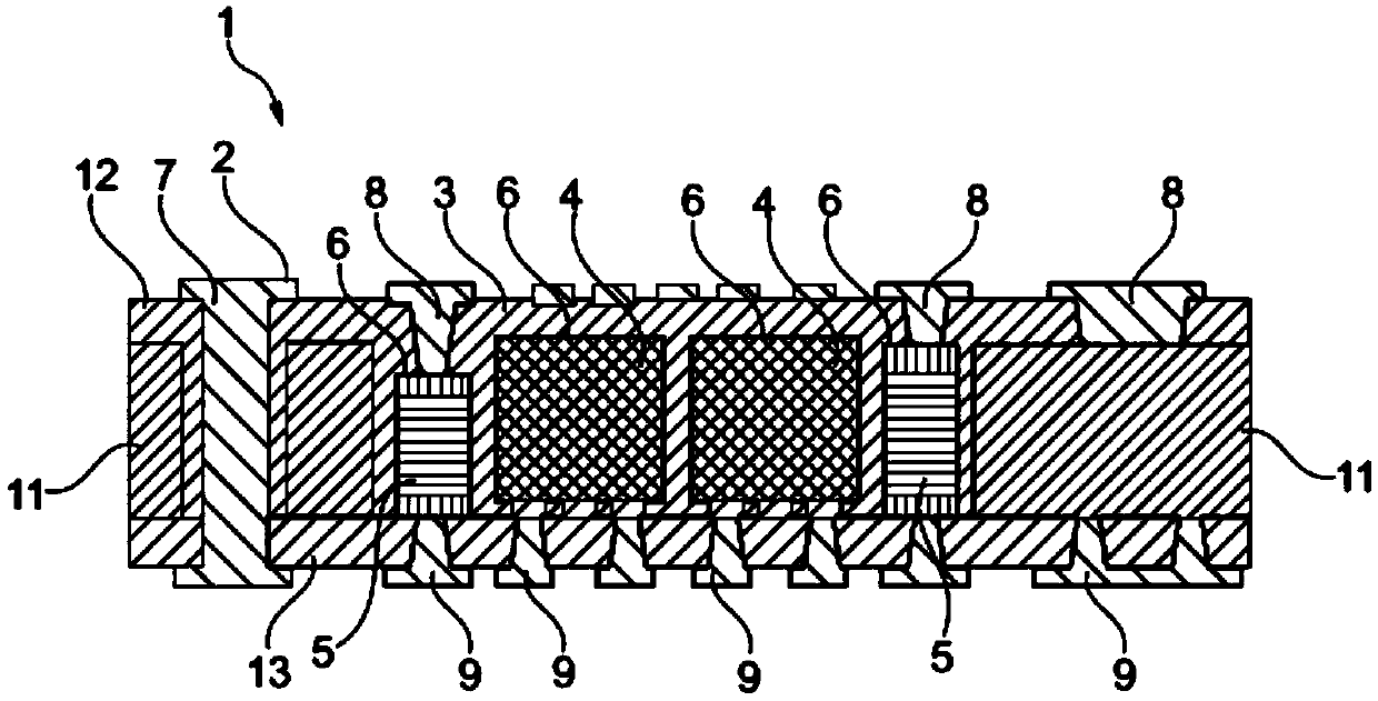
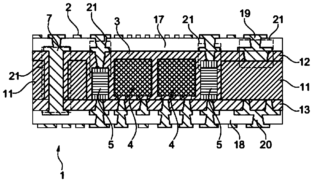
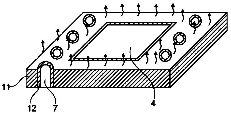
[0051] The illustrations in the figures are schematic. In different figures, similar or identical elements have the same reference signs.

[0052] Before describing the exemplary embodiments in more detail with reference to the accompanying drawings, some basic considerations upon which the exemplary embodiments of the present invention are developed will be summarized.

[0053] According to an exemplary embodiment, the nanocoating structure can be used in component carrier technology, in particular as a dry bonded structure. The adhesive layer that realizes this surface configuration can also be expressed as a gecko film. The adhesive effect of such surfaces can be based on van der Waals forces. Descriptively, multiple low-dimensional suction cups can be formed through such a concept. According to exemplary embodiments of the present invention, reliable substrates and / or structured materials are provided for embedded and / or surface mounted applications having specific adhe...


PUM


Abstract

The invention discloses a method for manufacturing a component carrier (1). The method comprises the steps of forming a stack including at least one electrically conducting layer structure (2) and / orat least one electrically insulating layer structure (3); patterning the front side of the stack with a first photo-imageable dielectric (PID) (12); and patterning the back side of the stack. The invention further discloses a component carrier (1).

Description

technical field [0001] The invention relates to a component carrier comprising a PID and to a method of producing the component carrier. Background technique [0002] An electronic device such as a computing device or a communication device typically includes at least one improved component carrier, such as a printed circuit board (PCB), an intermediate printed circuit board product or IC-substrate. In order to further enhance the interconnection characteristics and the density of electronic connections of such component carriers and reduce their size and thickness, components can also be integrated within the component carrier by means of the so-called Embedded Component Packaging (ECP) technology developed by the applicant . [0003] However, ECP substrates embedded with functional chips require thermal management to facilitate smooth chip operation, and additional processes such as pre-baking to prevent first-time lamination and component movement after UV impact to rem...

Claims


Application Information

Patent Timeline
IPC IPC(8): H01L21/56H01L23/31H01L23/367H01L23/48H01L25/16
CPCH01L25/16H01L23/3677H01L23/367H01L23/3135H01L23/481H01L21/56H01L2224/18H05K1/185H05K2203/0191H05K2201/10636H05K3/0023H05K3/0032H01L23/5389H01L23/5384H01L23/50H01L23/145H05K3/4608Y02P70/50H05K3/027H05K3/4644H05K3/0026H05K3/4038H05K3/007G03F7/26H05K1/115H05K1/05H05K1/0204H05K2203/107G03F7/20H05K1/186
Inventor 睦智秀
Owner AT & S AUSTRIA TECH & SYSTTECHN AKTIENGES
Why Eureka
Try Eureka