Electrostatic discharge immunity test method for processor chip

An electrostatic discharge and immunity technology, applied in the field of electrostatic discharge immunity test components, can solve the problems of no electrostatic discharge test standard, no standard for high-speed signal injection of integrated circuits, etc., to improve convenience and test efficiency. Effect

Active Publication Date: 2020-05-19
TIANJIN INST OF ADVANCED TECH +1
View PDF7 Cites 6 Cited by
  • Summary
  • Abstract
  • Description
  • Claims
  • Application Information

AI Technical Summary

Problems solved by technology

[0005] At present, most of the standards for integrated circuits are used for electronic components, and there are no electrostatic discharge test standards specific to IC pins, let alone a complete high-speed signal injection standard for integrated circuits.

Method used


Image

  • Electrostatic discharge immunity test method for processor chip
  • Electrostatic discharge immunity test method for processor chip
  • Electrostatic discharge immunity test method for processor chip

Examples


Embodiment 1

[0024] The present embodiment discloses a kind of ESD immunity testing assembly for processor chips, including: non-capacitance probes and capacitive probes respectively used to test the immunity of different pins of IC chips; and also including probe connections One end is used to connect the output end of the electrostatic discharge generator, and the other end is used to detachably connect the non-capacitive probe or the capacitive probe.

[0025] In this embodiment, the capacitance carried by the probe with capacitance is a coupling capacitance that can be connected in series between the probe connector and the single-ended signal pin of the high-speed DDR chip under test.

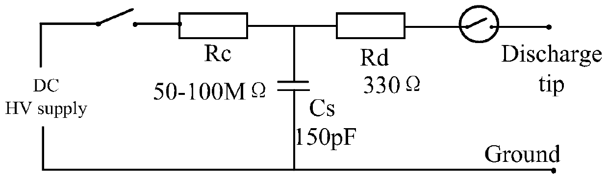
[0026] In this embodiment, it is equivalent to splitting the traditional system-level non-detachable probe into a probe connector and a non-capacitance probe. The circuit structure of the probe connector can be as follows: figure 1 circuit shown.

[0027] In the traditional IC ESD test, the ESD probe ...

Embodiment 2

[0042] Corresponding to the above component embodiments, this embodiment discloses an electrostatic discharge immunity test method for processor chips, including:

[0043] Step S1. Divide the pins of the tested IC chip into two types; one type is based on the non-capacitance probe for immunity test, and the other type is based on the capacitive probe for immunity test.

[0044] Step S2: Determine the type of the pin to be tested, and select the corresponding non-capacitance probe or probe with capacitance to connect to the electrostatic discharge generator via the probe connector for testing.

[0045] Preferably, the present embodiment method also includes:

[0046] Step S3, when measuring the single-ended signal of the high-speed DDR chip, select the probe with capacitance for testing, the capacitance carried by the probe with capacitance can be connected in series between the probe connector and the high-speed DDR chip under test Coupling capacitance between single-ended si...


PUM


Abstract

The invention relates to the technical field of integrated circuit detection and discloses a processor chip-oriented electrostatic discharge immunity test assembly and method so as to improve test fineness and convenience. The assembly comprises a non-capacitance probe and a capacitance probe which are respectively used for testing interference immunity of different pins of an IC chip, and a probeconnector, wherein one end of the probe connector is used for being connected with an output end of an electrostatic discharge generator, the other end of the probe connector is used for being detachably connected with the non-capacitance probe or the capacitance probe, a capacitor carried by the probe capacitor is a coupling capacitor which can be connected in series between the probe connectorand a single-ended signal pin of a tested high-speed DDR chip, the non-capacitance probe is used for connecting the probe connector with a pin of a differential signal of the high-speed DDR chip, andthe assembly further comprises a customized PCB test board which is provided with parallel coupling capacitors for the differential pins so as to be in butt joint with differential signal double-end pins of the tested high-speed DDR chip.

Description

technical field [0001] The invention relates to the technical field of integrated circuit detection, in particular to an electrostatic discharge immunity test component and method for processor chips. Background technique [0002] ESD (Electro-static discharge, electrostatic discharge) is a subject formed since the middle of the 20th century to study the generation, hazards and electrostatic protection of static electricity. It is customary in the world to refer to the equipment used for electrostatic protection as ESD. [0003] ESD test is electrostatic discharge test, which is used to verify the immunity of electronic and electrical equipment when it comes directly from the operator and electrostatic discharge to nearby objects. Because static electricity usually has a very high instantaneous voltage (greater than several thousand volts), it is the main culprit that causes electronic components or integrated circuits to cause excessive electrical stress (EOS: Electrical Ov...

Claims


Application Information

Patent Timeline
Patent Type & Authority Applications(China)
IPC IPC(8): G01R31/28G01R31/00
CPCG01R31/2884G01R31/2886G01R31/002
Inventor 吴建飞李雅菲张红丽郑亦菲李宏吴健煜王宏义郑黎明刘培国
Owner TIANJIN INST OF ADVANCED TECH
Why Eureka
Try Eureka