Flexible GaN-based MIS device applied to graphene and preparation method of flexible GaN-based MIS device

A technology of graphene and graphene layers, applied in the direction of semiconductor devices, electrical components, circuits, etc., can solve problems such as difficulty in achieving flexibility, light emission limitation, and reduced light extraction efficiency, and achieve low cost and easy-to-implement effects

Pending Publication Date: 2020-05-15
SUZHOU UNIV
View PDF0 Cites 1 Cited by
  • Summary
  • Abstract
  • Description
  • Claims
  • Application Information

AI Technical Summary

Problems solved by technology

MIS devices are mainly based on the relationship between carriers and bias applied to situations such as HEMT devices, plasma elements, MIS-LEDs, etc. At present, MIS devices based on GaN are mainly based on specific substrates such as Si, SiC or sapphire, etc. , it is difficult to achieve flexibility; secondly, the metal layer is mainly prepared by electroplating or sputtering metal, which will limit the light emission and greatly reduce the light extraction efficiency when applied to the MIS-LED structure

Method used


Image

  • Flexible GaN-based MIS device applied to graphene and preparation method of flexible GaN-based MIS device
  • Flexible GaN-based MIS device applied to graphene and preparation method of flexible GaN-based MIS device
  • Flexible GaN-based MIS device applied to graphene and preparation method of flexible GaN-based MIS device

Examples


Embodiment

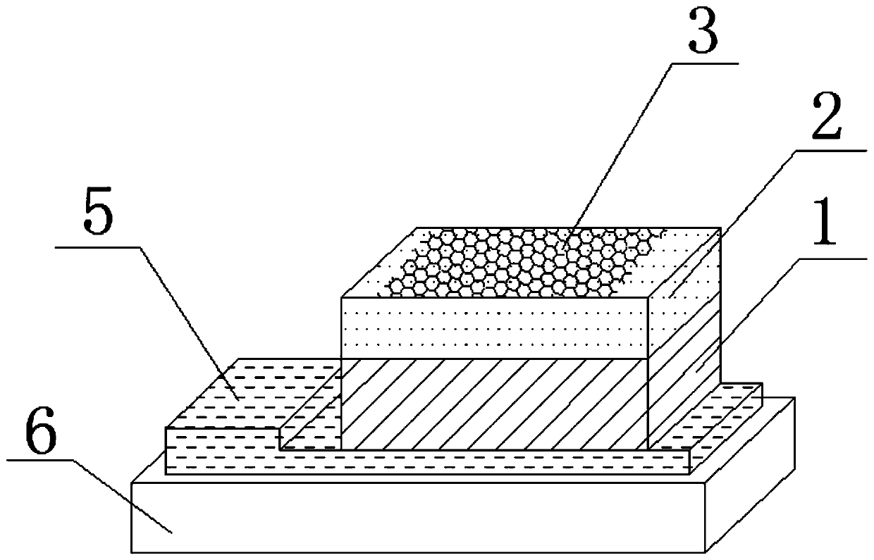
[0025] Such as Figure 1-3 Described, a kind of flexible GaN-based MIS device applied on graphene, comprises GaN film layer 1, AlN sputtering layer 2, graphene layer 3 and metal electrode layer, and described graphene layer 3 is positioned at AlN sputtering layer 2 Above, the AlN sputtering layer 2 wraps the graphene layer 3, and is located on the GaN film layer 1, and the GaN film layer 1 is located on the metal electrode layer, and the metal electrode layer includes a metal layer 5 and a substrate 6, so The metal layer 5 is plated on the substrate 6. The substrate 6 can be any substrate including a flexible substrate. In this embodiment, the substrate 6 is a flexible substrate wrapped with a high-temperature adhesive tape with a thickness of 4mm quartz rod.

[0026] The graphene layer 3 is multilayer graphene, and the number of layers is 5 layers.

[0027] The AlN sputtered layer 2 has a thickness of 10 nm and ensures high crystal quality, which is achieved by magnetron dep...


PUM

PropertyMeasurementUnit
Thicknessaaaaaaaaaa
Thicknessaaaaaaaaaa

Abstract

The invention discloses a flexible GaN-based MIS device applied to graphene. The flexible GaN-based MIS device comprises a GaN thin film layer, an AlN sputtering layer, a graphene layer and a metal electrode layer. The invention further discloses a preparation method of the flexible GaN-based MIS device applied to the graphene, the flexible GaN-based MIS device is prepared in an epitaxial growth mode, GaN serves as a semiconductor to provide local carriers, the AlN sputtering layer serves as a dielectric layer to achieve tunneling, and the graphene serves as a metal electrode to provide carriers acting with the semiconductor. The beneficial effects are that the preparation method is simple and easy to implement, has no special requirements for the substrate, can easily achieve flexibility,and can be placed on any flexible substrate and can be normally used, the performance of the GaN-based MIS device is basically not affected under the flexible condition, and the GaN-based MIS deviceand the preparation method are low in cost and easy to implement.

Description

technical field [0001] The invention relates to the technical field of semiconductor materials and devices, in particular to a flexible GaN-based MIS device applied on graphene. Background technique [0002] Gallium nitride (GaN) is one of the representatives of the third-generation wide-bandgap semiconductors. Its superior performance is high breakdown electric field, electron mobility, two-dimensional electron gas concentration and working ability under high temperature conditions. Gallium Nitride (GaN) material has a band gap of 3.4eV, and its intrinsic carriers at room temperature are very low, so devices tend to have very low leakage current. In addition, gallium nitride (GaN) materials have stable chemical properties, high temperature resistance, and corrosion resistance, and have inherent advantages in high-frequency, high-power, and radiation-resistant applications. Electronic devices based on AlN and GaN heterojunctions have achieved widespread application. The me...

Claims


Application Information

Patent Timeline
IPC IPC(8): H01L33/00
CPCH01L33/0037H01L33/007
Inventor 曹冰周浩王钦华
Owner SUZHOU UNIV
Why Eureka
Try Eureka