Image processing device and method, and display device

An image processing device and image processing technology, applied in image data processing, image enhancement, static indicators, etc., can solve the problems of increased chip power consumption, unfavorable battery life and battery life, and achieve the goal of reducing power consumption and preserving image quality Effect

Pending Publication Date: 2020-05-15
GIGADISPLAY SEMICON CO LTD +1
View PDF0 Cites 2 Cited by
  • Summary
  • Abstract
  • Description
  • Claims
  • Application Information

AI Technical Summary

Problems solved by technology

[0005] Under the above circumstances, in order to improve the display quality of the display device, the power consumption of the chip is increased, which is not conducive to the life and battery life of the battery.

Method used


Image

  • Image processing device and method, and display device
  • Image processing device and method, and display device
  • Image processing device and method, and display device

Examples


Embodiment Construction

[0053] Various embodiments of the invention will be described in more detail below with reference to the accompanying drawings. In the various drawings, the same elements are denoted by the same or similar reference numerals. For the sake of clarity, various parts in the drawings have not been drawn to scale.

[0054] In the description of the present application, the use of suffixes such as 'device', 'module' or 'unit' for denoting elements is only for facilitating the description of the present application and has no specific meaning by itself. Therefore, "device", "module", or "unit" may be used interchangeably.

[0055] The specific implementation manners of the present invention will be further described in detail below in conjunction with the accompanying drawings and embodiments.

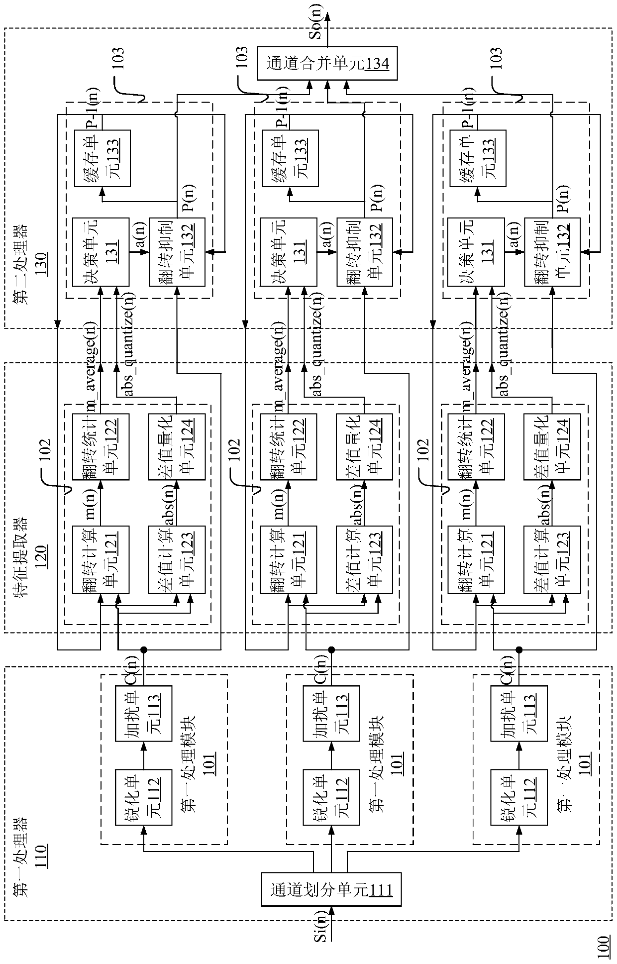
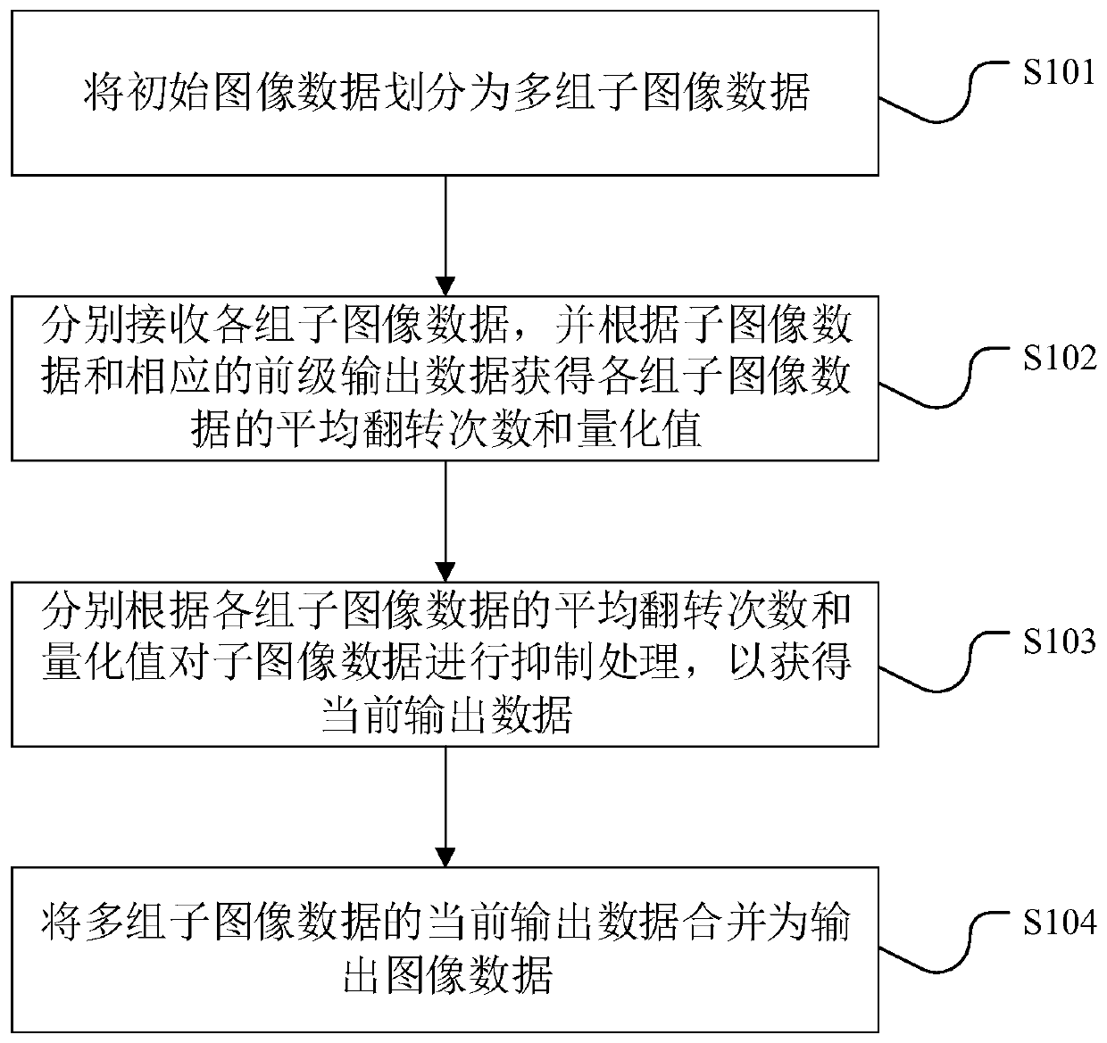
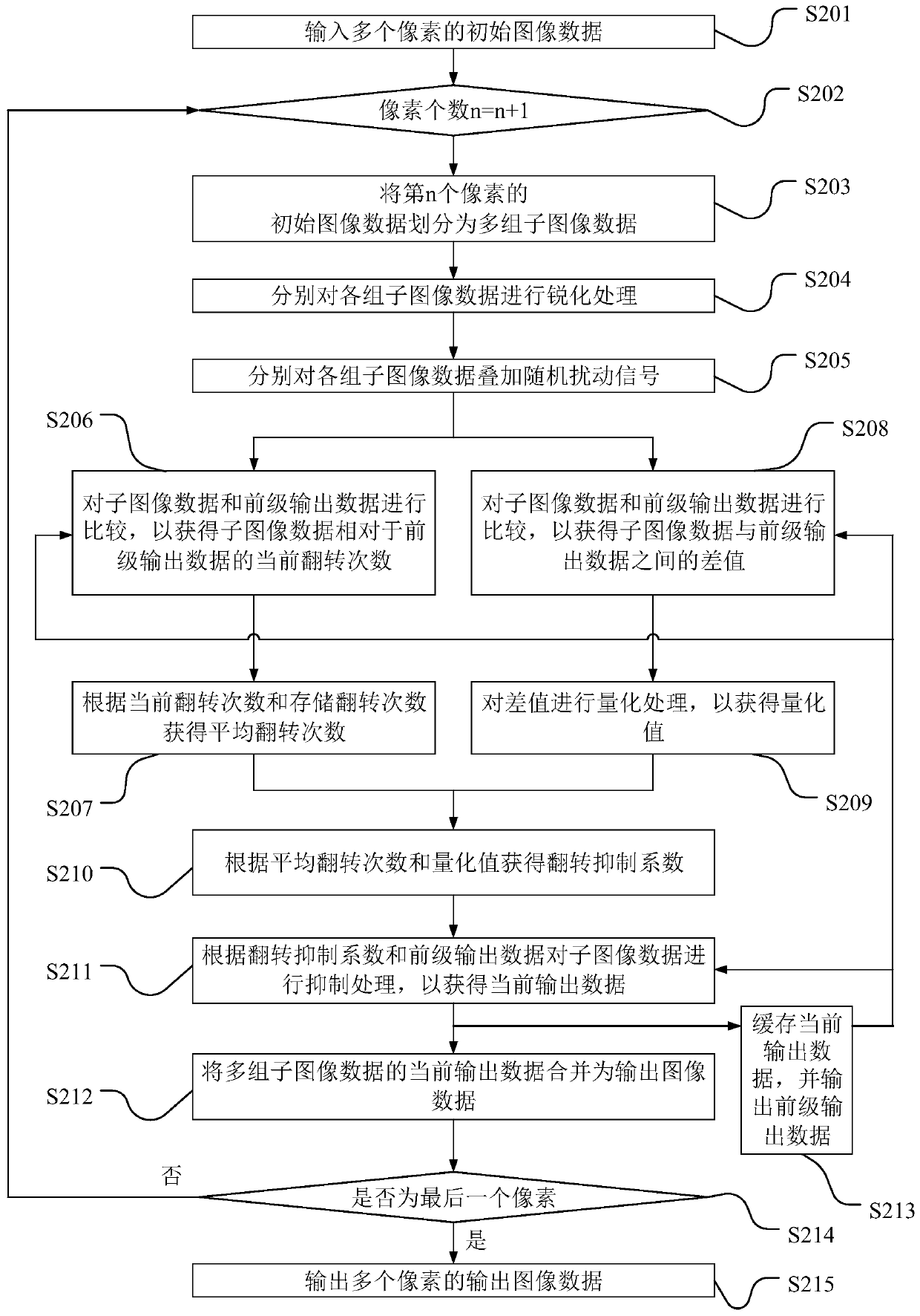
[0056] figure 1 A block diagram of an image processing apparatus according to an embodiment of the present invention is shown.

[0057] Such as figure 1 As shown, the image processing devi...


PUM


Abstract

The invention discloses an image processing device and a method, and a display device. The image processing apparatus includes: a first processor that divides initial image data into a plurality of groups of sub-image data; a feature extractor which is provided with a plurality of feature extraction modules which are used for receiving one group of the multiple groups of sub-image data respectively and obtaining the average turnover frequency and the quantized value of the sub-image data according to the sub-image data and the preceding-stage output data; a second processor which has multipleprocessing module, and each group of sub-image data is suppressed according to the average turnover frequency and the quantized value so as to obtain current output data, the second processor combinesthe multiple current output data output by the multiple processing modules into output image data, and the turnover frequency of the output image data is not greater than the turnover frequency of the initial image data. The image processing device suppresses the number of flipping times of output image data and reduces the overall power consumption of a post-stage system.

Description

technical field [0001] The present invention relates to the field of display technology, and more specifically, to an image processing device, method and display device. Background technique [0002] With the development of integrated circuit manufacturing technology and display technology, the requirements for image display in electronic products with display devices are getting higher and higher. For example, in the field of smart phone products, in order to provide finer display quality, the resolution of the display panel is getting higher and higher; in order to improve the smoothness of the display screen, the refresh frequency of the display panel is getting higher and higher. [0003] Currently, more and more display devices use Active Matrix Organic Light Emitting Diode (AMOLED) display panels. Compared with traditional Liquid Crystal Display (LCD) display panels, the display screen provided by AMOLED display panels It has many advantages such as fast response spee...

Claims


Application Information

Patent Timeline
IPC IPC(8): G06T5/00G09G3/3225
CPCG09G3/3225G06T5/73
Inventor 蔡剑田琪韩德栋王漪
Owner GIGADISPLAY SEMICON CO LTD
Why Eureka
Try Eureka