


Quick Research
Generate reliable direction feasibility study reports for your R&D in just a few steps.

Technical Q&A
Discover and master advanced knowledge NOW. Basics, ideas, possibilities, all at once.

Find Solutions
As an expert in R&D theories, this can generate solutions to your technical problems instantly.

Evaluate Feasibility
Analyze your overall solution with one click, know your potential R&D risks in advance.

Monitor Landscape
Get weekly tech updates, stay abreast of the latest tech innovations and key insights.
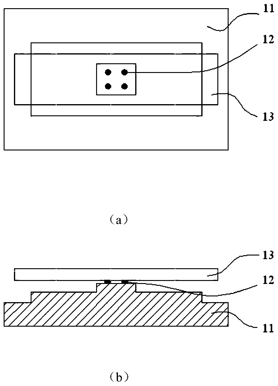
Method for realizing low-stress sensitive structure chip mounting process
A sensitive structure, low stress technology, applied in microstructure technology, microstructure devices, processing microstructure devices, etc., can solve the problem of affecting the accuracy index and environmental adaptability of MEMS devices, reducing the long-term reliability and stability of devices, and destroying MEMS. Device packaging atmosphere and other issues, to ensure long-term reliability and stability, low patch stress, and high integration.
- Summary
- Abstract
- Description
- Claims
- Application Information
AI Technical Summary
Problems solved by technology
Method used
Image


Examples
Embodiment Construction
[0030] It should be noted that, in the case of no conflict, the embodiments in the present application and the features in the embodiments can be combined with each other. The following will clearly and completely describe the technical solutions in the embodiments of the present invention with reference to the accompanying drawings in the embodiments of the present invention. Obviously, the described embodiments are only some, not all, embodiments of the present invention. The following description of at least one exemplary embodiment is merely illustrative in nature and in no way taken as limiting the invention, its application or uses. Based on the embodiments of the present invention, all other embodiments obtained by persons of ordinary skill in the art without creative efforts fall within the protection scope of the present invention.
[0031] It should be noted that the terminology used here is only for describing specific implementations, and is not intended to limit t...
PUM
 Abstract
Description
Claims
Application Information
 - R&D Engineer
- R&D Manager
- IP Professional
- Industry Leading Data Capabilities
- Powerful AI technology
- Patent DNA Extraction
Browse by: Latest US Patents, China's latest patents, Technical Efficacy Thesaurus, Application Domain, Technology Topic, Popular Technical Reports.
© 2024 PatSnap. All rights reserved.Legal|Privacy policy|Modern Slavery Act Transparency Statement|Sitemap|About US| Contact US: help@patsnap.com