
Scanning exposure apparatus

A scanning and equipment technology, applied in the field of scanning exposure equipment, can solve problems such as uneven luminescence

Inactive Publication Date: 2020-04-21
许铭案
View PDF1 Cites 0 Cited by
  • Summary
  • Abstract
  • Description
  • Claims
  • Application Information

AI Technical Summary

Problems solved by technology

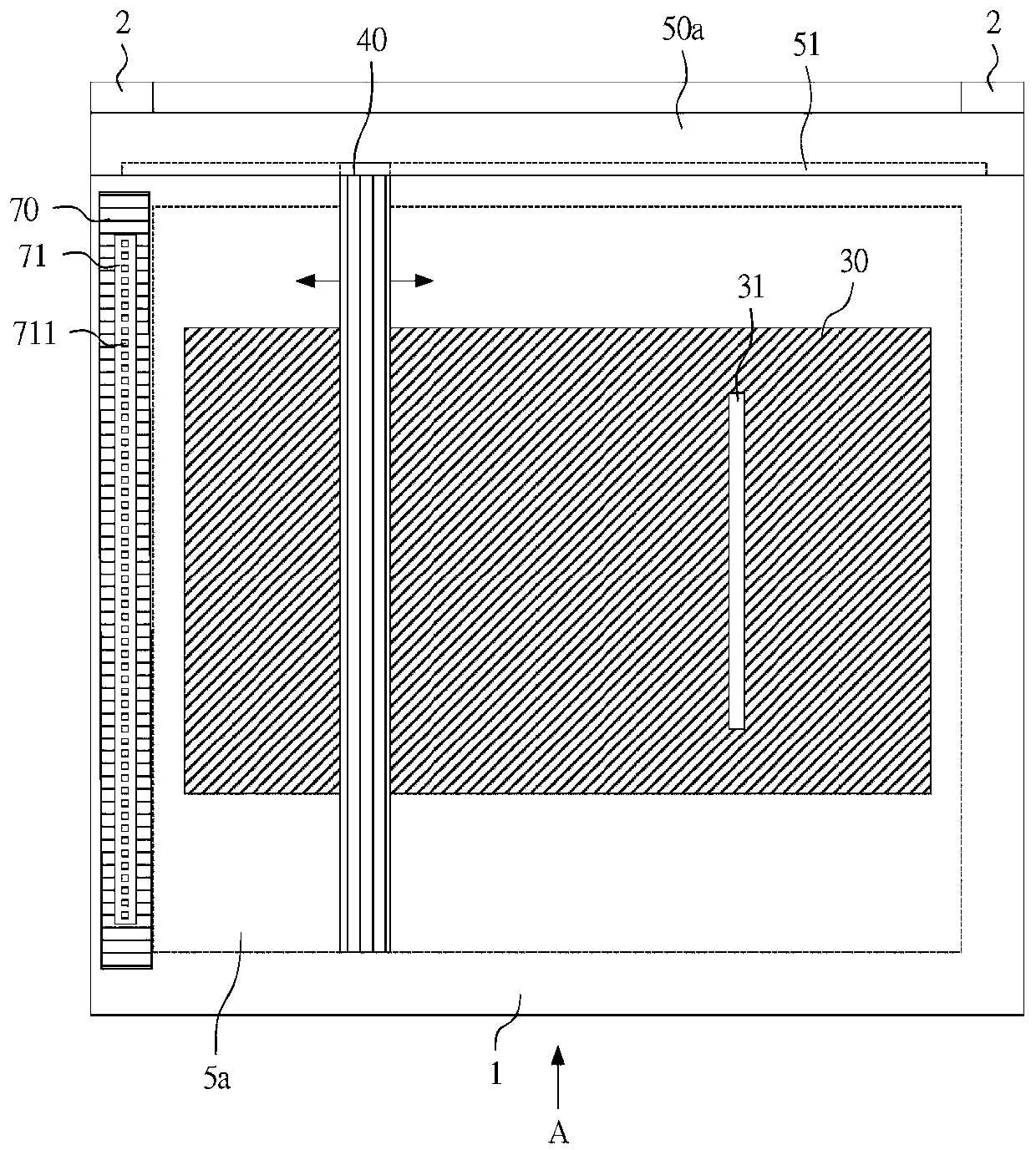
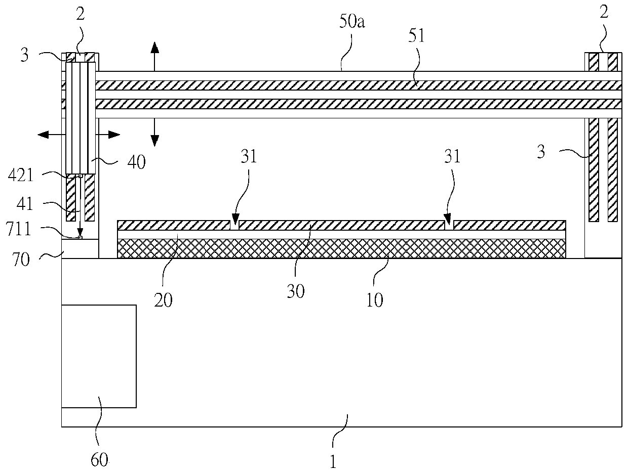
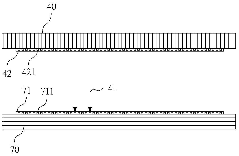
[0007] In order to achieve the above object, the present invention uses the first linear photoresistor arranged at the first end point (starting point) to detect the luminous conditions of individual LEDs among the linear LEDs in the linear light source, and then grasp their luminous intensity After that, correct it to the standard luminous intensity, which can effectively solve the technical problem of uneven luminous light that may be produced by linear light sources

Method used


Image

  • Scanning exposure apparatus
  • Scanning exposure apparatus
  • Scanning exposure apparatus

Examples


Embodiment Construction

[0017] According to an embodiment of the present invention, the present invention provides a scanning exposure device, which uses a linear light source that can provide linear collimated light, and then combines scanning technology to adjust the linear collimated light into collimated light that can scan the entire surface, No complicated optical mechanism is needed, and the equipment structure is simple, so that the purpose of greatly reducing the cost of exposure equipment can be achieved. In addition, the present invention uses the first linear photoresistor arranged at the first end point (starting point) to detect the light-emitting situation of individual light-emitting diodes among the linear light-emitting diodes in the linear light source, and then grasp its luminous intensity, and then adjust its Calibrating to the standard luminous intensity can effectively solve the technical problem of uneven luminous light that may be produced by linear light sources.

[0018] Pl...


PUM

PropertyMeasurementUnit
Wavelengthaaaaaaaaaa

Abstract

The invention discloses a scanning exposure apparatus, which comprises a base, a control circuit board, a linear light source, at least one transmission mechanism and at least one linear light detector, wherein the base is provided with a platform on which an assembly of a substrate and a photomask can be placed to perform a lithography process; the linear light source is electrically connected with the control circuit board and is provided with a plurality of light-emitting assemblies, the plurality of light-emitting assemblies can generate linear collimated light, and the linear collimated light is used for executing the lithography process; the at least one transmission mechanism is arranged on the base and connected with the control circuit board, the linear light source is arranged onone of the at least one transmission mechanism, and the at least one transmission mechanism can drive the linear light source to actuate; the at least one linear light detector consists of a plurality of photoresistors, is electrically connected with the control circuit board and is used for detecting the intensity of the linear light source; the control circuit board compensates the emission intensity of the plurality of light-emitting assemblies according to the intensity of the linear light source, so that the technical problem of non-uniform light emission possibly generated by the linearlight source can be effectively solved.

Description

technical field [0001] The present invention relates to an exposure device, in particular to a scanning exposure device for lithography process in the semiconductor industry. Background technique [0002] The lithography process is a basic equipment in the semiconductor industry, and it is the single largest cost factor in the cost of the semiconductor industry. According to an evaluation methodology published by Information Network Industries, the exposure system accounts for 20% of the total fab cost. The lithography equipment is mainly in the hands of optical equipment factories such as Nikon, ASML and SVGL. [0003] The exposure equipment in the lithography equipment currently adopts a one-time exposure method, and uses a complex optical mechanism to expose the aligned mask and substrate. This one-time exposure method needs to meet the requirements of light collimation, one-time (controllable time length) and the tight fit between the mask and the substrate, so the ali...

Claims


Application Information

Patent Timeline
IPC IPC(8): G03F7/20
CPCG03F7/70558G03F7/7085
Inventor 许铭案
Owner 许铭案
Learn More