Manufacturing method of circuit board with spot plating patterns

A manufacturing method and circuit board technology, which is applied in the direction of removing conductive materials by chemical/electrolytic methods, can solve problems such as ineffective filling, achieve good filling effects, increase yield, and improve the efficiency of post-processing

Active Publication Date: 2020-04-14
珠海杰赛科技有限公司 +1
View PDF6 Cites 0 Cited by
  • Summary
  • Abstract
  • Description
  • Claims
  • Application Information

AI Technical Summary

Problems solved by technology

For this reason, the present invention proposes a method for manufacturing circuit boards with dot-plating graphics, which can effectively solve the problem that the connection points between the steps of the existing dot-plating graphics and the lines cannot be effectively filled during film sticking, and improve the yield

Method used


Image

  • Manufacturing method of circuit board with spot plating patterns
  • Manufacturing method of circuit board with spot plating patterns
  • Manufacturing method of circuit board with spot plating patterns

Examples


Embodiment Construction

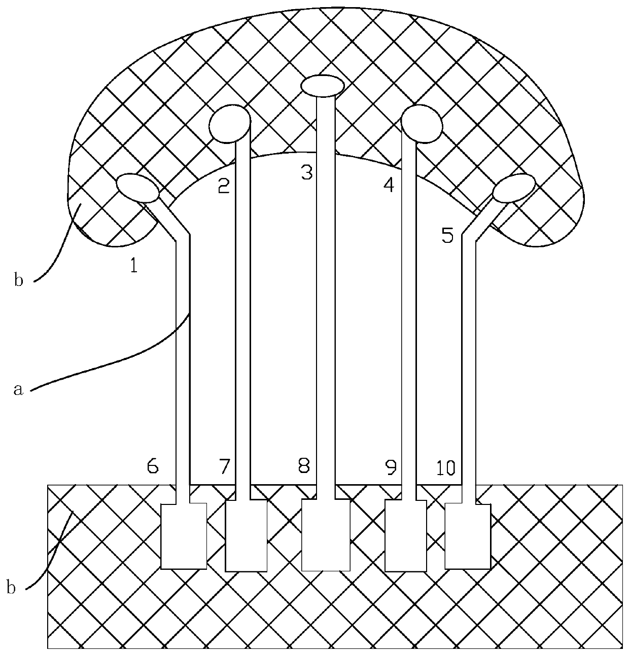
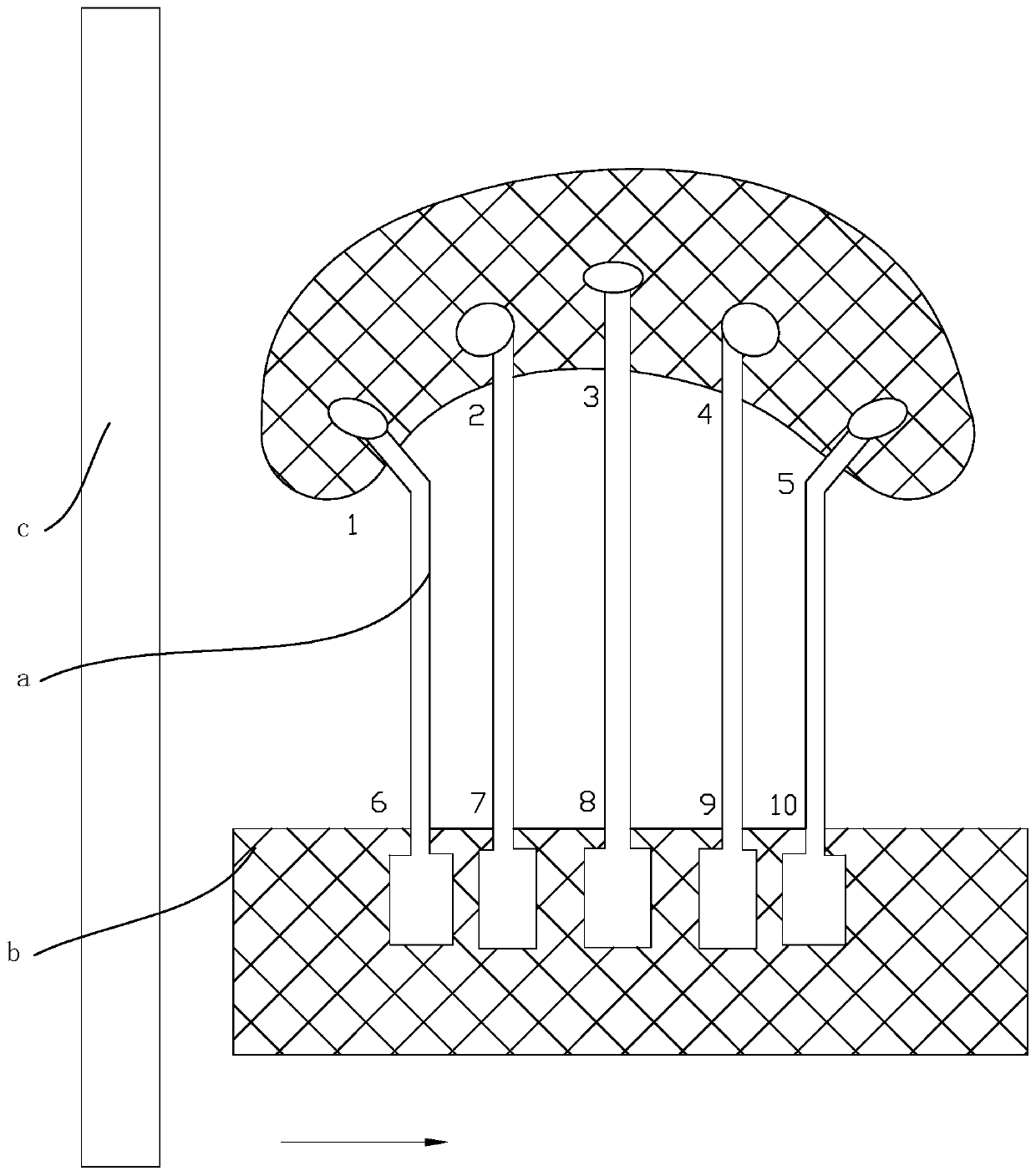
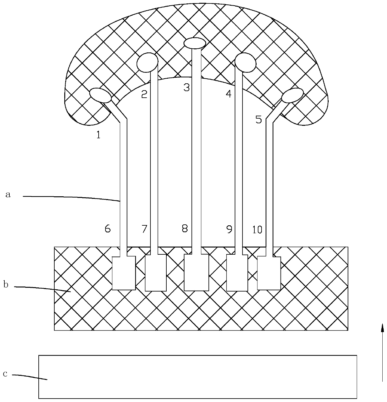
[0046] Embodiments of the present invention are described in detail below, examples of which are shown in the drawings, wherein the same or similar reference numerals designate the same or similar elements or elements having the same or similar functions throughout. The embodiments described below by referring to the figures are exemplary only for explaining the present invention and should not be construed as limiting the present invention.

[0047]In the description of the present invention, it should be understood that the orientation descriptions, such as up, down, front, back, left, right, etc. indicated orientations or positional relationships are based on the orientations or positional relationships shown in the drawings, and are only In order to facilitate the description of the present invention and simplify the description, it does not indicate or imply that the device or element referred to must have a specific orientation, be constructed and operated in a specific o...


PUM


Abstract

The invention discloses a manufacturing method of a circuit board with spot plating patterns. The method comprises the steps of pretreatment, copper deposition treatment, internal light imaging, spotplating, external light imaging and post-treatment. The method is characterized by roughening a surface of a copper layer in a micro-etching manner in spot plating, and obtaining rectangular spot plating patterns and circuits connected between the different spot plating patterns on a substrate; and electroplating the spot plating patterns and the circuits to a preset thickness in an electroplatingmode, wherein the spot plating patterns protrude out of the surface of a plate and form a rectangular step; and a rolling direction of a pressing roller on a laminator is parallel to a length direction of the step so as to compact connection areas of two ends of a line where a dry film is located and the step. By adoption of the manufacturing method, the thickened spot plating patterns are formedinto a regular pattern, in a secondary film pasting process, a joint between the spot plating patterns and the circuits is filled with the dry film in a specific film pasting mode, and a problem thatan open circuit and a short circuit are likely to happen to the joint between the spot plating patterns and the circuits in a later product machining process is solved.

Description

technical field [0001] The invention relates to the technical field of spot plating, in particular to a method for manufacturing a circuit board with spot plating patterns. Background technique [0002] With the rapid development of social economy and the optimization and upgrading of economic structure, it means that a new round of technological revolution and industrial transformation is emerging in the world, which is bound to have a profound impact on the manufacturing industry worldwide. As the basic components of electronic equipment, printed circuit boards are the transmission carriers of current and signals, and play a pivotal role in electronic equipment. Therefore, higher requirements are placed on printed circuit boards. [0003] In order to ensure quality, enhance customer confidence, speed up the development of potential customers, and strive for more market share to seize market opportunities, the process of printed circuit board design is more complicated, and...

Claims


Application Information

Patent Timeline
Patent Type & Authority Applications(China)
IPC IPC(8): H05K3/06
CPCH05K3/06
Inventor 刘顺风
Owner 珠海杰赛科技有限公司
Why Eureka
Try Eureka