Photovoltaic bypass diode in field of thin-film solar energy, and production process and installation method of photovoltaic bypass diode

A technology of bypass diodes and thin-film solar energy, which is applied in photovoltaic power generation, circuits, and final product manufacturing. Product reliability, firm and reliable structure, and high electrical yield

Pending Publication Date: 2020-03-27
山东芯诺电子科技股份有限公司
View PDF0 Cites 3 Cited by
  • Summary
  • Abstract
  • Description
  • Claims
  • Application Information

AI Technical Summary

Problems solved by technology

With the development of new thin-film solar energy technology, the demand for bypass diodes for thin-film solar panels is increasing, while the existing thin-film solar energy bypass diodes such as Figure 1-3 As shown, the photovoltaic diode 16 is packaged in TO-277, and the packaged diode is combined with a welding extension wire. The client needs to manually weld the extension lead for the photovoltaic diode. After welding, it is assembled with the thin film solar panel, and the process is cumbersome.
The product body is too thick, affecting customer use
The edge of the device is too sharp, it is easy to scratch the protective film on the back of the component, causing product damage
The welding effect of the discrete device and the frame will directly affect the performance of the component. The yield rate of manual welding is not high, which can no longer fully meet the needs of customers.
[0003] like Figure 4 As shown, when installing TO-277 packaged photovoltaic diodes, the installation is cumbersome - when using the original product, the customer needs to manually weld the extension leads for the photovoltaic diodes, and then assemble with the thin film solar panel after welding, the process is more cumbersome
The effect of welding the discrete device and the frame will directly affect the performance of the component, and the yield rate of manual welding is not high
The sharp corners during the installation of the components will scratch the film covering the surface of the solar panel, causing damage to the product

Method used


Image

  • Photovoltaic bypass diode in field of thin-film solar energy, and production process and installation method of photovoltaic bypass diode
  • Photovoltaic bypass diode in field of thin-film solar energy, and production process and installation method of photovoltaic bypass diode
  • Photovoltaic bypass diode in field of thin-film solar energy, and production process and installation method of photovoltaic bypass diode

Examples


Embodiment 1

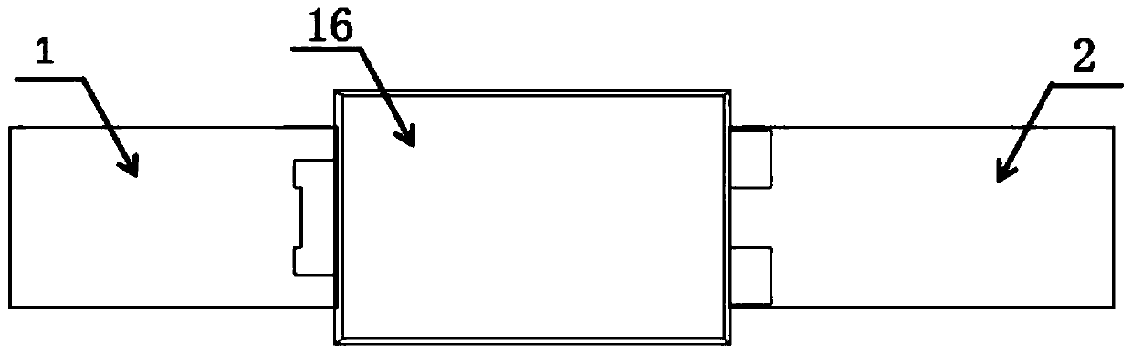
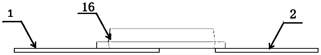
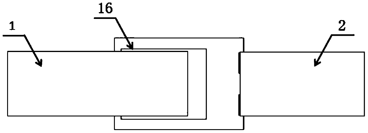
[0058] Such as Figure 5-10 As shown, the photovoltaic bypass diode in the field of thin film solar energy according to the present invention includes a diode body, and the diode body includes a diode negative lead terminal 1 and a diode positive lead terminal 2, and a diode negative lead terminal 1 and a diode positive lead terminal 2 are provided with Diode chip 9, a bonding jumper 11 is connected above the diode chip 9, one end of the bonding jumper 11 is connected to the top of the diode chip 9, and the other end is connected to the diode anode lead 2, wherein the diode chip 9 is placed on the diode cathode On the lead end 1, the diode cathode lead end 1 is connected to the diode anode lead end 2 through the diode chip 9 and the bonding jumper 11, and a chip mounting surface 8 is provided below the diode chip 9, and the diode chip 9 is placed above the chip mounting surface 8 , the bottom surface of the diode chip 9 is combined with the chip mounting surface 8, the diode c...

Embodiment 2

[0075] On the basis of Embodiment 1, the photovoltaic bypass diode also includes a frame, and several photovoltaic bypass diodes are arranged on the frame, and frames 17 are arranged on the upper and lower sides of the frame, and the upper and lower sides of the photovoltaic bypass diode are all connected with the frame set up and down. 17 connections, the photovoltaic bypass diodes are evenly arranged in a matrix on the frame, and support ribs 18 are arranged between multiple photovoltaic bypass diodes, and the support ribs 18 are connected to the positive and negative leads on the photovoltaic bypass diodes, so that the current passes through the surface of the frame .

[0076] The manufacturing process of the present invention adopts a matrix copper frame, and a single chip can accommodate 48 diode units, which improves the utilization rate of the frame and saves copper consumption. At the same time, due to the use of ultra-thin plastic packaging, the use of plastic packagin...

Embodiment 3

[0079] Such as Figure 11 As shown, the production process of the photovoltaic bypass diode in the field of thin film solar energy of the present invention comprises the following steps:

[0080] Step 1: Raw material preparation:

[0081] Prepare frame, diode chip, solder paste and molding material;

[0082] Step 2 Mounting and welding:

[0083] The assembly adopts automatic assembly of welding wires, distributing solder such as solder paste on the frame, then sucking and placing the diode chip 9 to the designated position of the frame, distributing solder paste on the surface of the diode chip 9, and then placing the bonding jumper 11 on the designated position position, let the diode chip 9 and the chip mounting surface 8 form a special connection circuit, and finally, solder, so that the above components form an integral circuit;

[0084] Step 3: Ultrasonic Cleaning:

[0085] Ultrasonic vibration cleaning is used to remove various residues and contamination after weldin...


PUM


Abstract

The invention discloses a photovoltaic bypass diode in the field of thin-film solar energy, production process thereof and an installation method thereof. The invention belongs to the technical fieldof semiconductor electrical components. The diode comprises a diode cathode lead end and a diode anode lead end. A diode chip is arranged between the diode cathode lead end and the diode anode lead end, a bonding jumper wire is connected above the diode chip, the diode chip is placed on the diode cathode lead end, the diode cathode lead end is connected with the diode anode lead end through the diode chip and the bonding jumper wire, a frame chip mounting surface is arranged below the diode chip, a diode plastic package body is arranged outside the diode chip, and a back plate cooling fin is arranged at the position, corresponding to the frame chip mounting surface, of the back surface of the diode body. A photovoltaic diode and an extension lead which are separated in an original productare integrated together, and a client element welding procedure is replaced. And the heat dissipation capability of the element is remarkably enhanced in an integrated packaging mode of the element.

Description

technical field [0001] The invention relates to a photovoltaic bypass diode in the field of thin-film solar energy, a production process and an installation method thereof, and belongs to the technical field of semiconductor electrical components. Background technique [0002] Photovoltaic bypass diodes are widely used in solar power generation equipment, and are usually connected in parallel and reversely between the positive and negative electrodes of solar cell modules. Under abnormal conditions, it can protect the safety of photovoltaic power generation components, minimize power loss, and maintain the normal operation of photovoltaic power generation devices. With the development of new thin-film solar energy technology, the demand for bypass diodes for thin-film solar panels is increasing, while the existing thin-film solar energy bypass diodes such as Figure 1-3 As shown, the photovoltaic diode 16 is packaged in TO-277, and the packaged diode is combined with welding...

Claims


Application Information

Patent Timeline
Patent Type & Authority Applications(China)
IPC IPC(8): H01L31/0443H01L31/0445H01L31/18H01L23/367H01L23/495
CPCH01L23/367H01L23/495H01L31/0443H01L31/0445H01L31/1876Y02E10/50Y02P70/50
Inventor 姜旭波吴南郝龙翠
Owner 山东芯诺电子科技股份有限公司
Why Eureka
Try Eureka