
Display panel and driving method

A driving method and display panel technology, applied to static indicators, instruments, etc., can solve the problems affecting the picture quality of micro-light-emitting diode displays, the decrease of picture contrast, and the large number of micro-light-emitting diodes, etc., so as to improve the picture display effect and improve the picture quality. Contrast ratio, power saving effect

Active Publication Date: 2020-03-27
INTERFACE TECH CHENGDU CO LTD +2
View PDF14 Cites 2 Cited by
  • Summary
  • Abstract
  • Description
  • Claims
  • Application Information

AI Technical Summary

Problems solved by technology

[0003] Although the reverse bias current is very small, but the number of micro light emitting diodes on the display panel is large, the reverse bias current direction of each micro light emitting diode is the same, and after accumulation, a large sum of reverse bias currents can be formed. The sum of the bias currents will affect the picture quality of the micro-LED display, resulting in a decrease in picture contrast

Method used


Image

  • Display panel and driving method
  • Display panel and driving method
  • Display panel and driving method

Examples


Embodiment 1

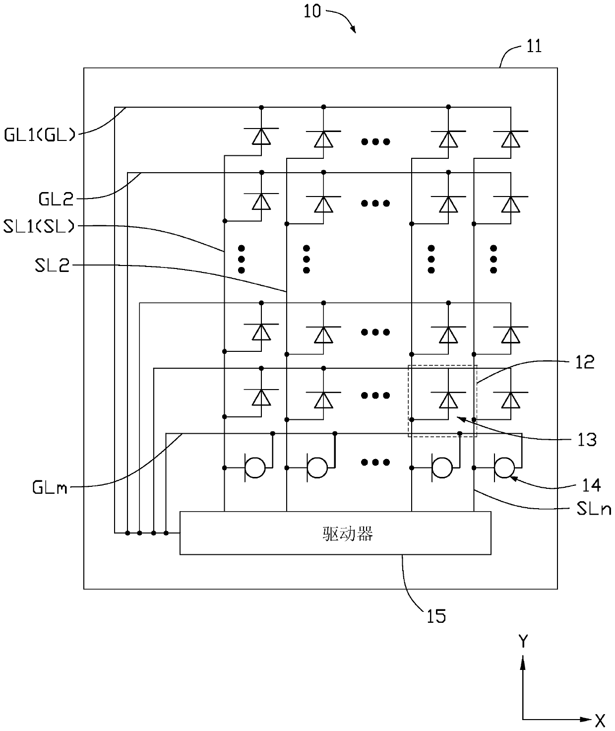
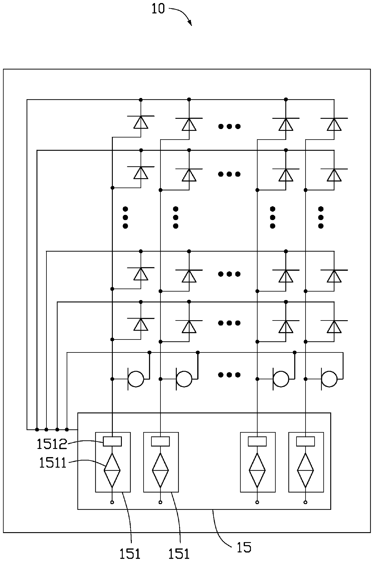
[0044] see figure 1 The display panel 10 provided in this embodiment includes a substrate 11, m gate lines (GL1˜GLm, m>2) and n data lines (SL1˜SLn, n>2) formed on the substrate 11, each The gate lines are arranged in parallel with each other at intervals, and the data lines are arranged in parallel with each other. The m gate lines and the n data lines are insulated from each other and cross each other to define a plurality of sub-pixels 12 arranged in an array, such as figure 1 As shown in , the X direction is defined as the row direction of the sub-pixel array, and the Y direction is defined as the column direction of the sub-pixel array.

[0045] read on figure 1 , the display panel 10 further includes a plurality of LEDs 13 disposed on the substrate 11 , and each LED 13 is located in a sub-pixel 12 . Each light emitting diode 13 has an anode and a cathode, the anode of each light emitting diode 13 is electrically connected to the gate line GL defining the sub-pixel 12 w...

Embodiment 2

[0077] The structure of the display panel provided in this embodiment is basically the same as that of the display panel 10 in Embodiment 1, and will not be repeated here. see Figure 12 The main difference between the driving method provided in this embodiment and the first embodiment is that, before step S3, it also includes:

[0078] Step S4, judging the reverse bias current i of the non-working light-emitting diode 13 electrically connected to the data line SL1 r Whether the sum is less than the target drive current i of the light emitting diode 13 in the working state electrically connected to the data line SL1 R ;

[0079] If it is judged as yes, step S5 is executed to control the current source 14 to open;

[0080] If the judgment is negative, step S6 is executed to control the current source 14 to be turned off.

[0081] In this embodiment, the current source 14 is not continuously turned on during the working process of the display panel 10, but according to the r...


PUM


Abstract

The invention provides a display panel, which comprises m gate lines which are arranged at intervals along a first direction; n data lines which are arranged at intervals in the second direction, wherein the m gate lines and the n data lines are insulated and crossed to define a plurality of sub-pixels; a plurality of light emitting diodes, each light emitting diode being formed in one sub-pixel and electrically connected to one data line and one gate line, and having a reverse bias current in a non-working state; n current sources, each current source having an output current, each current source being formed in a sub-pixel, each current source being electrically connected to a data line and a gate line, respectively, and each current source being connected to a different data line; and adriver electrically connected with the m gate lines and the n data lines, wherein the driver is used for controlling the working states of each light-emitting diode and each current source and controlling reverse bias current and output current to drive the light-emitting diode in the working state at present to emit light. The invention further provides a driving method.

Description

technical field [0001] The present invention relates to the technical field of image display, in particular to a display panel and a driving method applied to the display panel. Background technique [0002] In the prior art, a micro light emitting diode display defines a plurality of pixel areas arranged in an array on the display panel, each pixel area includes a plurality of sub-pixels, each sub pixel is provided with a micro light emitting diode, and a driving signal is output through a driver To each micro-light emitting diode, each micro-light-emitting diode can be controlled to light up or turn off, and through the light-emitting coordination of each micro-light-emitting diode, the micro-light-emitting diode display can display different images. Among them, the micro light emitting diode has the characteristics of "forward conduction and reverse cut off", that is, if the anode voltage of the micro light emitting diode is higher than the negative voltage and the positi...

Claims


Application Information

Patent Timeline
Patent Type & Authority Applications(China)
IPC IPC(8): G09G3/32
CPCG09G3/32
Inventor 陈忠君庄胜钧周蔣云陈伯纶
Owner INTERFACE TECH CHENGDU CO LTD
Learn More