Array substrate and preparation method thereof, and display panel

An array substrate and substrate substrate technology, which is applied in semiconductor/solid-state device manufacturing, semiconductor devices, electrical components, etc., can solve problems such as uneven display screen, poor TFT stability, and start-up voltage drift.

Active Publication Date: 2022-08-09
BOE TECH GRP CO LTD +1
View PDF6 Cites 0 Cited by
  • Summary
  • Abstract
  • Description
  • Claims
  • Application Information

AI Technical Summary

Problems solved by technology

The structure of the display panel in the prior art is as figure 1 as shown, figure 1 Only the base substrate 1, the light shielding layer 2, the buffer layer 3, the semiconductor region 4 of the active layer, the gate insulating layer 5 and the gate 6 are shown, from figure 1 It can be seen from the figure that the semiconductor region 4 of the active layer is easily affected by the light irradiated from the side, resulting in poor stability of the TFT, easy to cause the phenomenon of start-up voltage drift, and resulting in uneven display
[0003] To sum up, in the display panel of the prior art, the semiconductor region of the active layer of the thin film transistor is easily affected by light, and the start-up voltage drift is prone to occur, resulting in poor stability of the TFT, resulting in uneven display images, and affecting the display effect.

Method used


Image

  • Array substrate and preparation method thereof, and display panel
  • Array substrate and preparation method thereof, and display panel
  • Array substrate and preparation method thereof, and display panel

Examples


Embodiment Construction

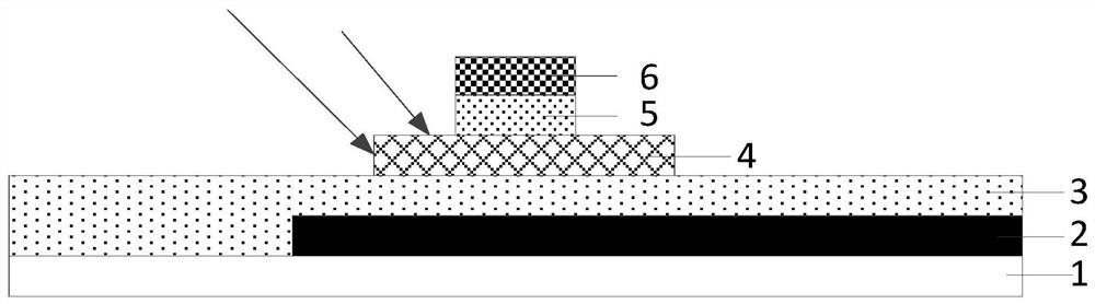
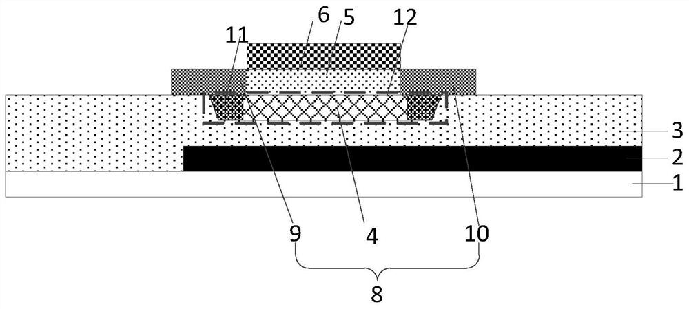
[0063] The embodiments of the present application provide an array substrate, such as figure 2 As shown, the array substrate includes: a base substrate 1, a light shielding layer 2 located on the base substrate 1, a buffer layer 3 located on the light shielding layer 2, and a buffer layer 3 located on the buffer layer 3 The source layer 8, and the light shielding part 11; the buffer layer 3 has a groove 12;

[0064] The active layer 8 includes: a semiconductor region 4, and a first conductive region 9 and a second conductive region 10 of the semiconductor region 4;

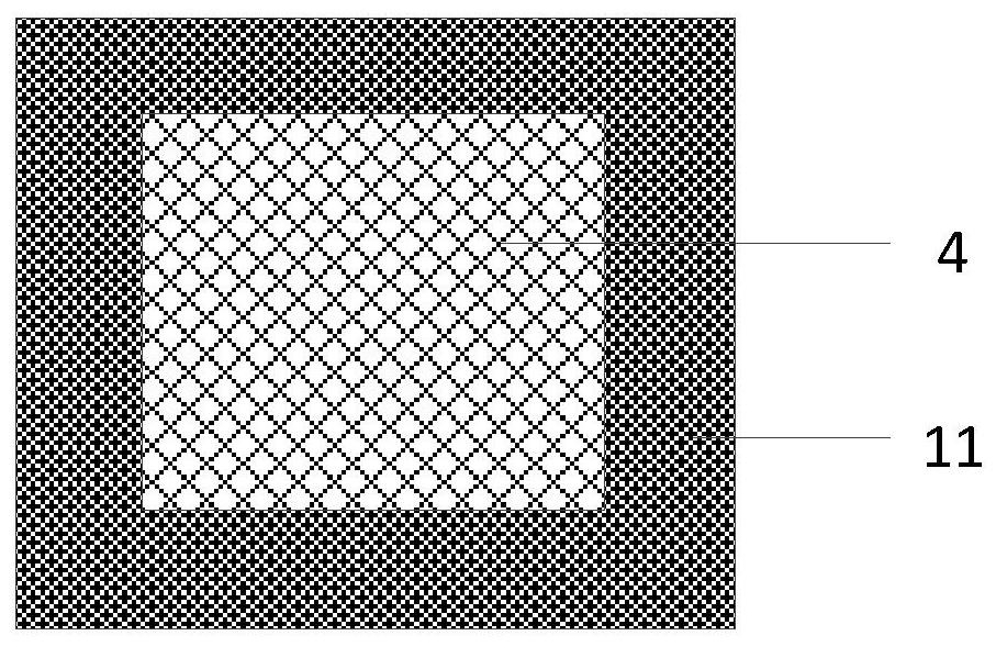
[0065] The semiconductor region 4 and the light shielding portion 11 fill the groove 12; such as image 3 As shown, the shape of the orthographic projection of the light shielding portion 11 on the base substrate 1 is annular, the side surface of the semiconductor region 4 is completely surrounded by the light shielding portion 11, the first conductive region 9 and the The second conductive region 10 is located...


PUM


Abstract

The present application discloses an array substrate, a preparation method thereof, and a display panel, which are used to prevent the semiconductor region of the active layer of the thin film transistor from being exposed to light, improve the working stability of the thin film transistor, avoid uneven display images, and improve the display effect. The array substrate provided by the present application includes: a base substrate, a light-shielding layer on the base substrate, a buffer layer on the light-shielding layer, an active layer on the buffer layer, and a light-shielding portion; the buffer layer has a groove; The active layer includes: a semiconductor region, a first conductive region and a second conductive region connected to the semiconductor region; the semiconductor region and the light shielding portion fill the groove; the shape of the orthographic projection of the light shielding portion on the substrate is annular, and the semiconductor region The side surface of the shading portion is completely surrounded by the shading portion, and the first conducting region and the second conducting region are located on the shading portion and the semiconductor region; the orthographic projection of the light shielding layer on the base substrate covers the orthographic projection of the semiconductor region on the base substrate.

Description

technical field [0001] The present application relates to the field of display technology, and in particular, to an array substrate, a preparation method thereof, and a display panel. Background technique [0002] At present, organic light-emitting diode (Organic Light-Emitting Diode, OLED) display products have the advantages of large screen brightness, wide color gamut, low power consumption, and large viewing angle, and have been vigorously developed. OLED display panels include thin film transistors (Thin Film Transistor, TFT), and TFTs in pixel circuits usually use oxide semiconductor materials as active layers, such as indium gallium zinc oxide (Indium Gallium Zinc Oxide, IGZO). The prior art display panel structure is as follows figure 1 shown, figure 1 Only the base substrate 1, the light shielding layer 2, the buffer layer 3, the semiconductor region 4 of the active layer, the gate insulating layer 5 and the gate electrode 6 are shown, from figure 1 It can be se...

Claims


Application Information

Patent Timeline
Patent Type & Authority Patents(China)
IPC IPC(8): H01L27/12H01L29/786H01L27/32H01L21/84H01L21/34
CPCH01L27/1218H01L27/1222H01L27/1244H01L27/1255H01L27/1259H01L27/1262H01L27/127H01L27/1288H01L29/78633H01L29/66969H10K59/12
Inventor 王海涛黄勇潮汪军苏同上李广耀王东方
Owner BOE TECH GRP CO LTD
Why Eureka
Try Eureka