Method for post-processing light absorption layer of Cu-based thin film solar cell and depositing buffer layer
A technology for thin-film solar cells and light-absorbing layers, applied in circuits, photovoltaic power generation, electrical components, etc., can solve problems such as Zn diffusion difficulties, performance degradation of thin-film solar cells, and obstacles to the marketization process, and achieve improved surface composition and morphology , Weaken the effect of light infiltration and improve the performance
- Summary
- Abstract
- Description
- Claims
- Application Information
AI Technical Summary
Problems solved by technology
Method used
Image

Examples
preparation example Construction
[0052] The specific embodiment of the present invention also provides a method for preparing a thin film solar cell, comprising the following steps:
[0053] (1) depositing a back electrode layer on the substrate, and depositing a light absorbing layer on the back electrode layer;
[0054] (2) using the post-processing method in the above-mentioned embodiment to process the light-absorbing layer;
[0055] (3) Depositing a buffer layer Zn(O,S) on the light absorbing layer by using the method in the above embodiment;
[0056] (4) Depositing a window layer on the buffer layer Zn(O,S), and forming a gate on the window layer.
[0057] Preferably, the substrate is soda-lime glass; the back electrode is Mo, and the light absorption layer can be formed by co-evaporation in three steps.
[0058] Preferably, the window layer is magnesium-doped zinc oxide (ZnMgO) and aluminum-doped zinc oxide (Al:ZnO), which can be deposited by magnetron sputtering.
[0059] Preferably, the grid is a ...
Embodiment 1
[0062] The aftertreatment method of the light absorbing layer of CIGS thin film solar cell comprises the steps:
[0063] (1) Aqueous ammonia solution is configured, and the concentration of the aqueous ammonia solution is 1M;
[0064] (2) Place the CIGS light-absorbing layer in the ammonia solution in such a way that the surface to be treated of the light-absorbing layer is perpendicular to the liquid level of the ammonia solution, heat the solution to 65° C., and perform etching treatment for 5 minutes;
[0065] (3) Take out the treated CIGS light-absorbing layer, wash it with deionized water, dry it with gas, and store it in vacuum for future use.
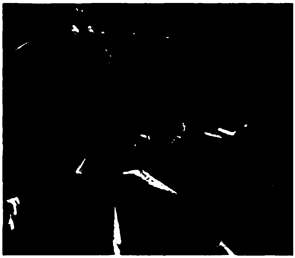
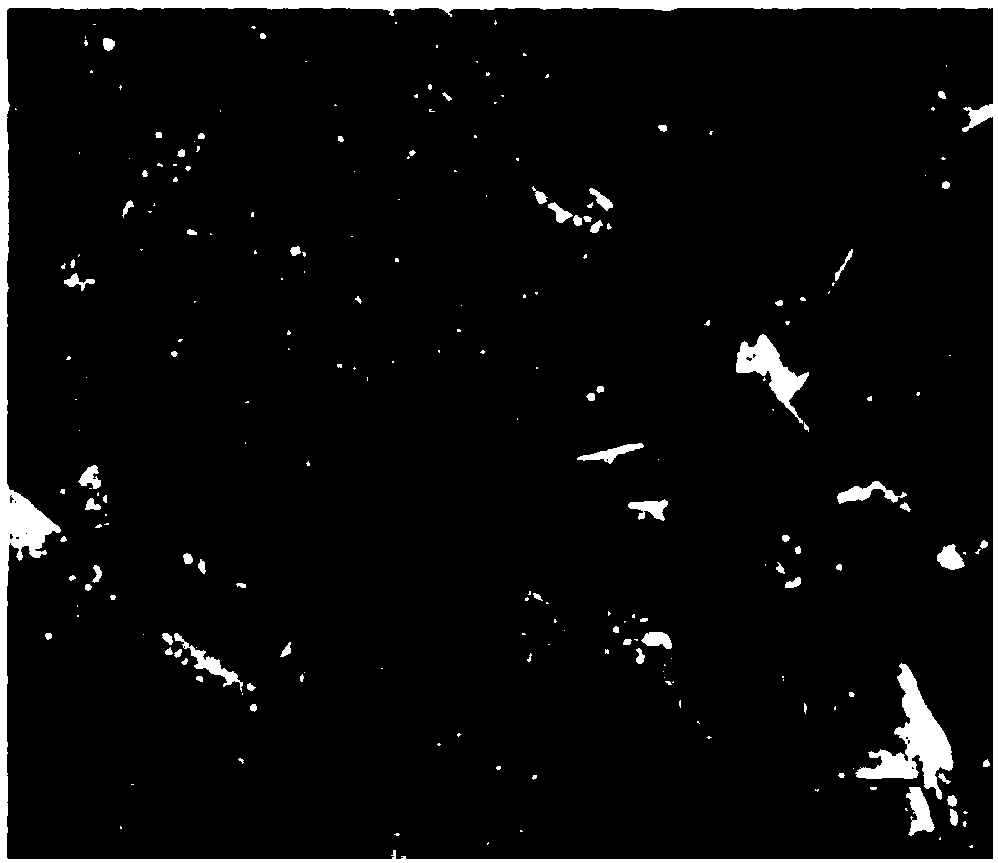
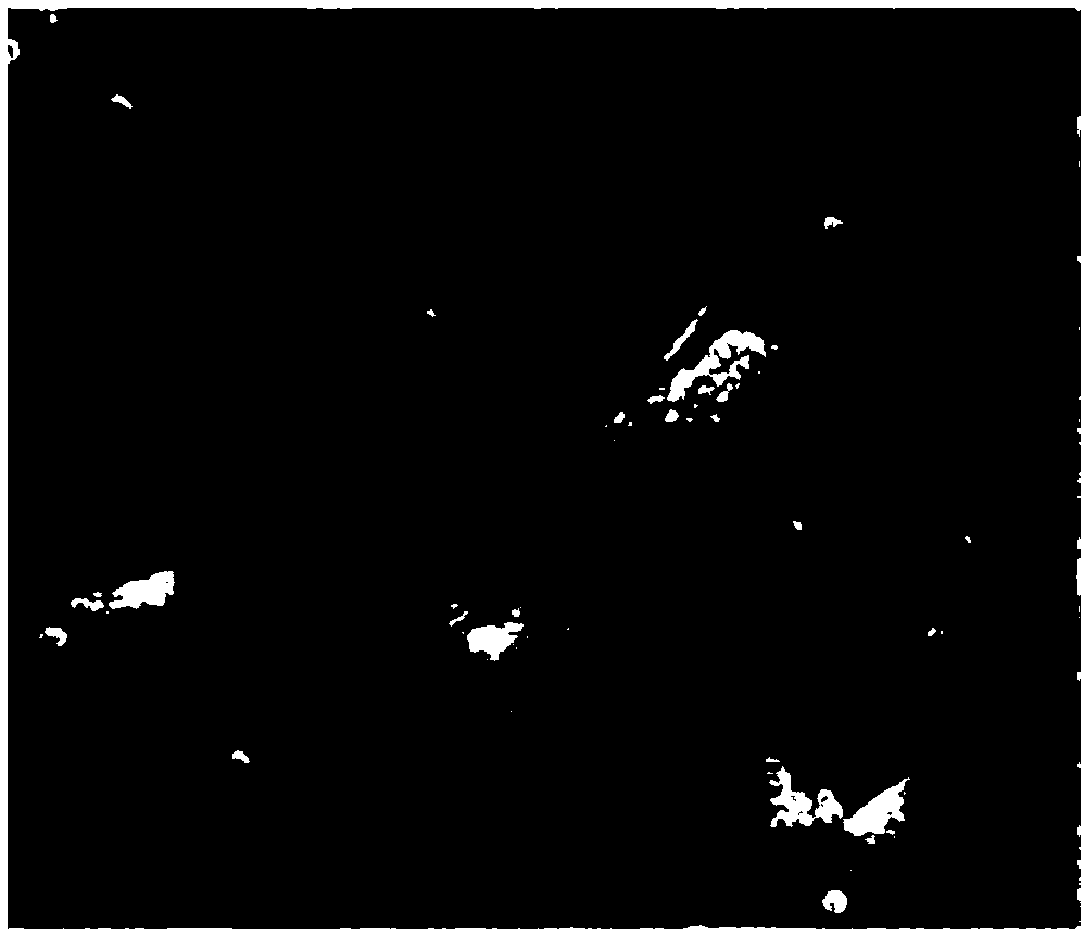
[0066] After the above treatment, the surface composition and morphology of the CIGS light absorption layer can be improved. Such as Figure 1a with 1b Shown are the SEM images of the untreated CIGS light-absorbing layer and the SEM image of the above-mentioned CIGS light-absorbing layer; it can be seen from the figure that the...
Embodiment 2
[0068] The method for depositing buffer layer Zn (O, S) on the light absorbing layer of CIGS thin film solar cell comprises the steps:
[0069] (1) First mix and stir the zinc acetate solution and the citric acid solution for 5 minutes, then add the thioacetamide solution and the ammonia solution and mix and stir for 30 seconds at the same time to obtain a deposition solution. In the deposition solution, Zn 2+ concentration of 7.5mM, the concentration of citric acid was 6.5mM, S 2- The concentration is 7.5mM, the concentration of ammonia water is 1.4M;
[0070] (2) Immerse the CIGS light-absorbing layer processed by the post-treatment method of Example 1 in the deposition solution, and deposit a buffer layer Zn (O, S) on the light-absorbing layer by heating in a water bath. The temperature and temperature of the water-bath heating can be adjusted. The thickness of the buffer layer Zn(O,S) is controlled by the heating time and the amount of the precursor substance. In this exa...
PUM
 Abstract
Description
Claims
Application Information
 - Generate Ideas
- Intellectual Property
- Life Sciences
- Materials
- Tech Scout
- Unparalleled Data Quality
- Higher Quality Content
- 60% Fewer Hallucinations
Browse by: Latest US Patents, China's latest patents, Technical Efficacy Thesaurus, Application Domain, Technology Topic, Popular Technical Reports.
© 2025 PatSnap. All rights reserved.Legal|Privacy policy|Modern Slavery Act Transparency Statement|Sitemap|About US| Contact US: help@patsnap.com